HDI PCB: Smaller, Faster, and Denser
for Modern Technologies
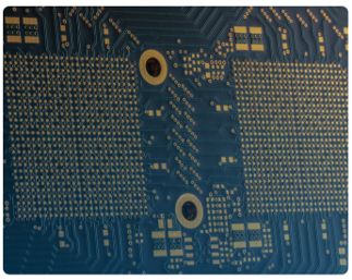
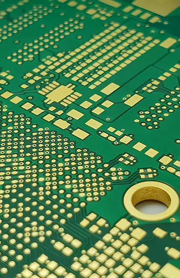
High-Density Interconnect, or HDI PCB, are using microvias and smaller trace/space to provide a higher signal density and superior signal integrity. It enables the interconnection of low-pitch packages and much higher component population density.
Product Benefits
HDI PCB improves the fan out and reduces the signal path length. It also removes via stubs and reduces reflections of signals, thus improving signal quality.

Better Signal Integrity
HDI helps in placing the components closer to each other which cuts down the signal path length. It removes via stubs, reduces reflections of signals, and thus improves signal quality.

High Reliability
Laser-drilled microvias have less chance of manufacturing mistakes and interconnecting defects during PCB production compared with conventional via PTHs (plated through holes). The microvias are also less affected by CTE (Coefficient of Thermal Expansion) during the assembly process.

Cost-Effective
Although the square meter price is higher for HDI PCBs, the superior signal integrity, higher reliability, and space, weight, and layer savings make HDI PCBs a cost-effective quality solution.
What are HDI PCB?
Definition
HDI: High-Density Interconnect. There are many different definitions of HDI technology. Common for all HDI boards is the use of smaller trace & space and microvias to create higher wiring routing density than a conventional PCB.


Specifications
Line and Space: HDI PCBs typically have smaller trace and spacing widths with sizes as small as 0.002, 0.003, or 0.004 inches (50, 75, 100 microns). Most manufacturers use laser direct imaging (LDI) and vacuum Develop-Etch-Strip (DES) lines to etch fine patterns.
Vias: Laser-drilled micro-vias and buried vias are used to increase the number of interconnections required for modern low-pitch BGA component density.
Layer Count: Reduced layer distance used in most HDI PCBs helps to reduce the PCB thickness and weight of the final product.
PCB Material: We normally recommend using mid or high Tg. material for HDI PCBs. Many applications with controlled trace impedances require special high-speed materials with low dissipation factor (Df) & low relative dielectric constant (εr Dk)
Surface Finish: For the assembly of an HDI PCB, a flat solder pad surface with good solderability is required. The most common finishes used are OSP ENIG, ENEPIG, and Immersion Sn.
Do you need HDI PCBs?
HDI is a necessity when the component pitch requires it, or the board size demands it. When properly designed, HDI PCBs are smaller, thinner, and weigh less (board downsizing trend). HDI has a myriad of constructions and variables that all affect density. To understand how blind vias, skip vias, staggered vias, stacked vias, and buried vias contribute to density, you must do a “routing test” and play with all these different stack-ups and constructions. By measuring the metrics (inches/square inch and pins/square inch), you can create a table that relates these density measures to the corresponding construction.
HDI PCB design techniques are used when considering the need to mount extreme component density on a limited board size. The component density determines the number of connections per square inch of the board. If the connections of all the parts and test points divided by the size of the board are less than 120 — 130 pins per square inch, there is no need to be using HDI, unless the use of specific dense BGA requires HDI to facilitate all connections. HDI technology has revolutionized the electronics industry and is used in most electronic gadgets you know. The demand for Printed Circuit Board using HDI technology looks promising for many various industries.
Technical Data
HDI
| HDI Feature | ICAPE Group HDI technical specification |
|---|---|
| Layer count | Up to 24 layers standard. Advanced 36 layers. |
| Technology highlights | High Density Interconnection PCB with laser blind holes. POFV (Plated Over Filled Via), till 4 sequential laminations (N+4). Advanced N+6, ELIC (Every Layer Interconnect) 14 Layers (X-Via). |
| Materials | FR4 raw material with high TG, low CTE, halogen-free, Hi-Speed and low loss specifications |
| Base Copper Thickness | 1/3 Oz to 2 Oz |
| Minimum track & spacing | 0.075mm / 0.075mm, Advanced 0,075mm / 0,05mm |
| Surface finishes available | OSP, ENIG, ENEPIG, Soft-Gold, Gold fingers, Immersion Tin, Immersion Silver. Advanced slective OSP / ENIG |
| Minimum laser drill | 0.10mm. Advanced 0,05mm |
| Minimum mechanical drill | 0.125mm. Advanced 0,1mm |
| PCB thickness | 0.40mm – 3,2mm, Advanced 5mm. |
| Maxmimum dimensions | 525x680mm. Advanced: 980x360mm. |
Learn more about HDI

Webinars on Demand - HDI
If you’ve missed a webinar, we now offer various webinars on demand, available upon request!

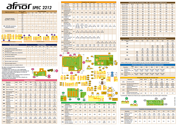
AFNOR PCB Design Guide
AFNOR SPEC 2212 is a benchmark specification developed to address the growing need for robust, sustainable, and forward-thinking solutions in PCB design

Technologies
Learn about the different technologies in the PCB industry and find which one suits your needs best.
Any questions?
There is an ICAPE Group team close to you and your business. All around the world, our business units are staffed with native experts available to answer all your questions.
Contact us today!
