IC Substrate Technology:
Next-Gen Ultra HDI PCB Innovations
IC Substrate, like PCB (SLP), is pushing the boundaries between HDI PCB technology and IC substrate technology. SLP is an integrated part of the IC packaging or module used to connect the chip with the PCB motherboard. SLP Technology development is mainly driven by the mobile phone and wearable electronic device industries, and it is a rapidly growing market.
Product Benefits
The main functions of the IC substrate board include chip soldering and electrical connection by wire bonding or flip chip process, and it guarantees reliability by using adapted raw material for chip elongation. Reliability is guaranteed by using raw materials adapted to the elongation of the different materials during the assembly phases and climatic constraints.

High Density
Substrate Like PCB (SLP) brings HDI PCB production to a new level with ultra-fine line/space down to 30/30µm. Common roadmaps of the SLP Manufactories expect to reach line/space 20/20µm in 2024 and 10/10 in 2025.

Reliability
Substrate Like PCB (SLP) is based upon BT (Bismaleimide Triazine) resin material instead of FR4. The BT material has a very high Tg. 250 to 300°C and a very low X&Y CTE 2-5 ppm/°C instead of 11-14 ppm/°C for FR4. This ensures very reliable integration with the IC substrates and creates the possibility to create Modules or Systems in Packages (SIP) with chips or components with high-density design.

Performance
SLP technology uses high-performance materials, the process of the IC Substrate and the stack-ups with laser defined vias known from HDI technology to create a very reliable and ultra complex HDI PCB.
What is IC Substrate PCB?
Definition
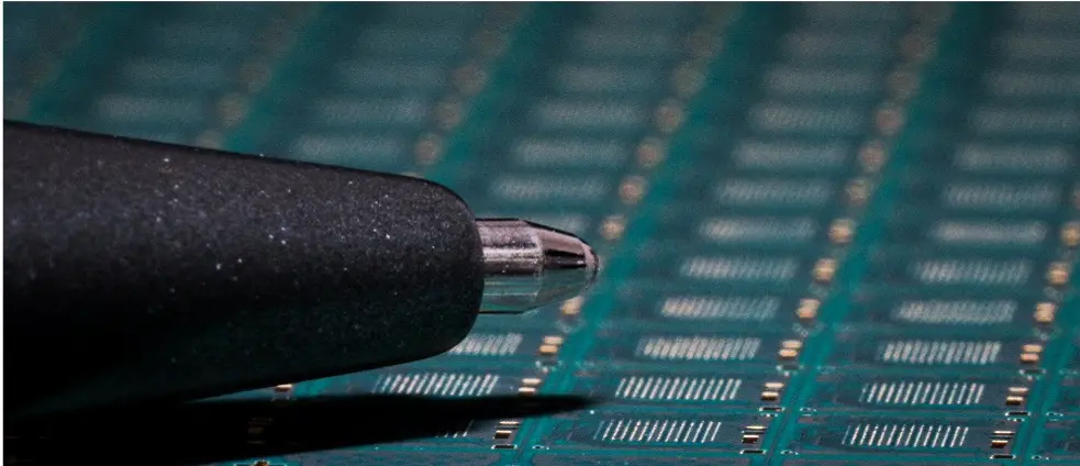
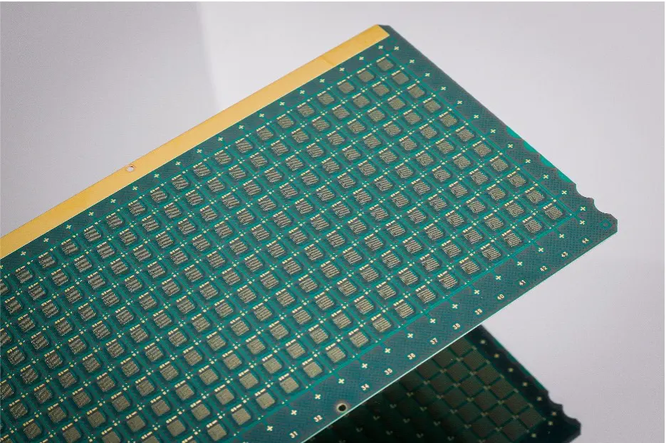
An IC substrate-like PCB (SLP), also known as an IC carrier board, is a type of printed circuit board that is specifically designed to hold integrated circuit (IC) chips. It is an ultra HDI PCB used in the semiconductor industry to package and connect IC chips to the rest of the electronic system.
The main function of an IC substrate PCB is to provide a physical platform for mounting and interconnecting the IC chips. The SLP typically has 2-6 layers of conductive traces, laser-defined vias, and pads that allow for electrical connections between both the IC chips and the PCB.
Specifications
Line and space: 30/30µm (advanced 20/20µm)
Vias: 50µm Laser defined.
Layer count: 2 to 6
PCB material: BT resin, Bismaleimide Triazine
IC Substrate Structure
There are 3 different process methods.
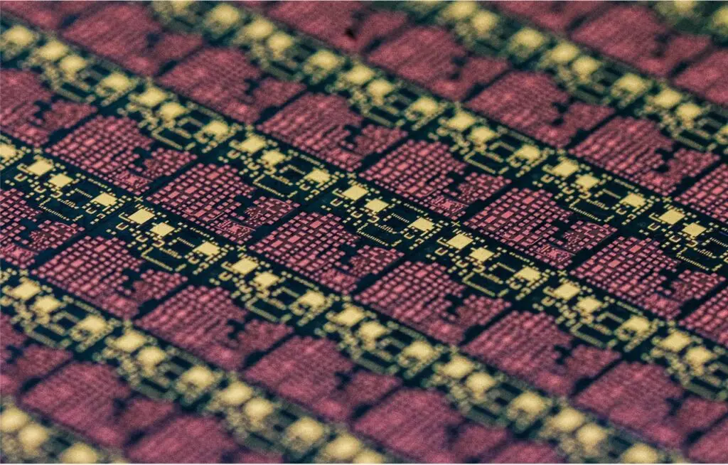
Subtractive method – a subtractive process using thin copper sheets of 9–12 µm and production steps based on the panel tenting method.
mSAP – A modified semi-additive process: a modified semi-additive process using an ultra-thin 1.5 µm copper foil, chemical copper plating + selective copper plating and selective etching.
SAP – Semi-additive process: a semi-additive process using a special material without a copper base and a chemical copper plating + selective copper plating and selective etching. 15/15µm Line & Space possible. (The SAP method can create up to 12 layers, but it is only available for mass production.)
IC Substrate Stack-up and material
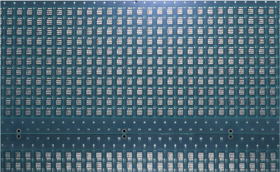
Stacking similar to HDI PCBs with core and PP.
BT (Bismaleimide Triazine) resin material instead of FR4
BT it’s higher Tg. 250 to 300°C
BT it’s lower CTE XY axis 2-5ppm/°C instead of 11-14ppm/°C for FR4.
Limited to stack-up 2L, 4L, and 6L for standard and 1+2+1, 1+4+1, 2+2+2 for structure.
Do you need IC Substrate PCB's?
Double-sided and multilayer PCBs are commonly used in a wide range of electronic applications such as telecommunications, industrial control systems, and power supplies. They are also used in prototyping and small-scale production runs.
Technical Data
IC Substrate
| HDI Feature | ICAPE Group IC Substrate technical specification |
|---|---|
| Layer count | 2 to 6 |
| Technology highlights | IC Substrate is PCB support for 1 Chip solder by Wire Bonding Process or Flip Chip Process |
| Materials | BT (Bismaleimide Triazine) |
| Base Copper Thickness | 0-12um depending upon substrate structure method |
| Minimum track & spacing | 30/30µm (Advanced 20/20µm) |
| Surface finishes available | ENIG & ENEPIG |
| Minimum laser drill | 50µm |
| Minimum mechanical drill | 100µm |
| PCB thickness | 2L min. 130µm, 4L min. 210µm, 6L min. 300µm |
Learn more about IC Substrate
Webinars on Demand
If you’ve missed a webinar, we now offer various webinars on demand, available upon request!
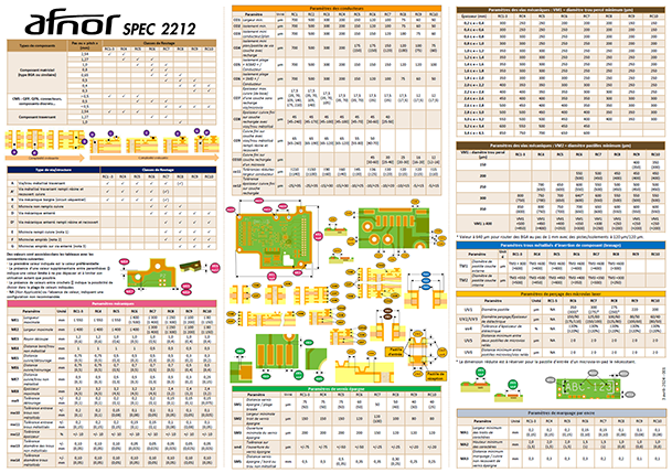
AFNOR PCB Design Guide
AFNOR SPEC 2212 is a benchmark specification developed to address the growing need for robust, sustainable, and forward-thinking solutions in PCB design
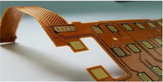
Technologies
Learn about the different technologies in the PCB industry and find which one suits your needs best.
Any questions?
There is an ICAPE Group team close to you and your business. All around the world, our business units are staffed with native experts available to answer all your questions.
Contact us today!
