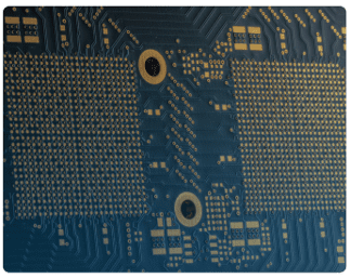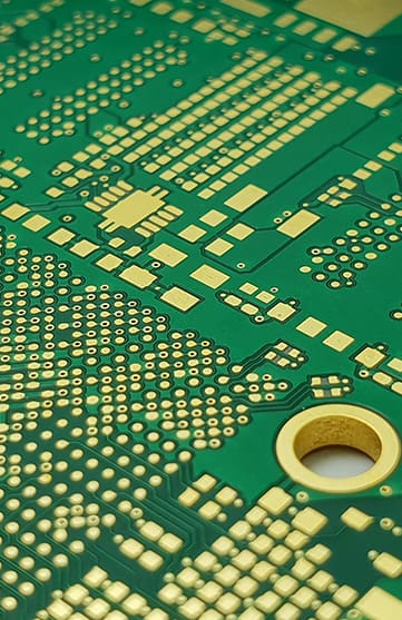
Better Signal Integrity
HDI helps in placing the components closer to each other which cuts down the signal path length. It removes via stubs, reduces reflections of signals, and thus improves signal quality.

High Reliability
Laser-drilled microvias have less chance of manufacturing mistakes and interconnecting defects during PCB production compared with conventional via PTHs (plated through holes). The microvias are also less affected by CTE (Coefficient of Thermal Expansion) during the assembly process.

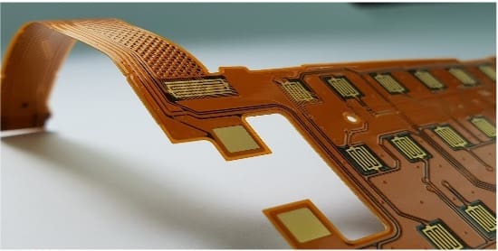
Cost-Effective
Although the square meter price is higher for HDI PCBs, the superior signal integrity, higher reliability, and space, weight, and layer savings make HDI PCBs a cost-effective quality solution.