Printed Circuit Boards (PCBs) have been the backbone of modern electronic devices for decades. As technology advances, the demand for smaller, lighter, and more efficient devices grows. PCB microvias play a crucial role in meeting these demands. This comprehensive guide will explore the world of PCB microvias, their types, manufacturing processes, applications, and essential design considerations. Whether you are a seasoned PCB designer or a curious enthusiast, this article will unravel the miniature marvels that power the electronics of the future.
What are PCB Microvias?
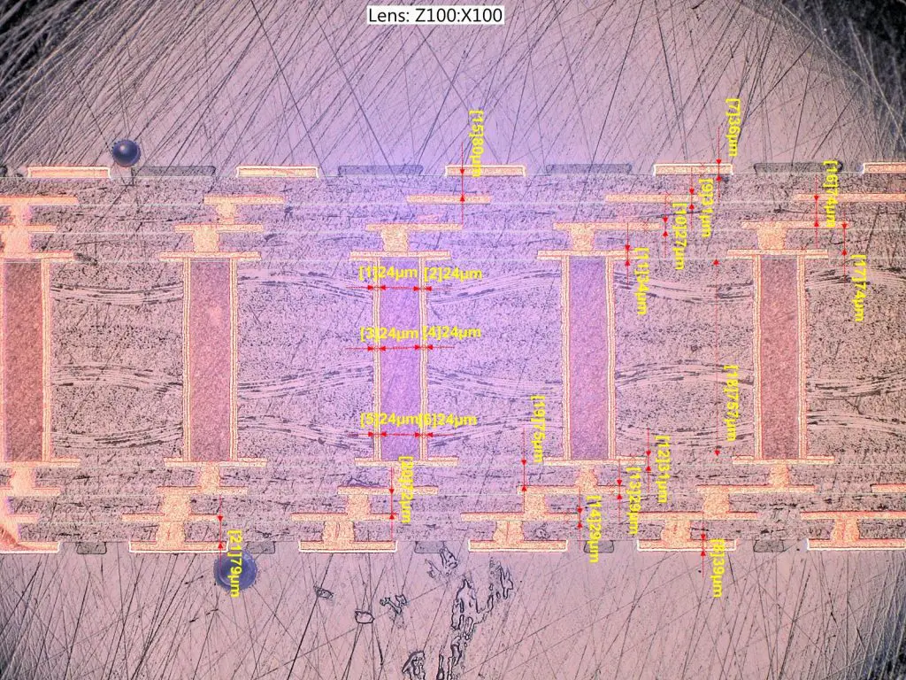
Microvias are tiny holes that traverse one or more layers of a PCB, typically with diameters ranging from 0.1mm to 0.15mm. These microscopic wonders act as pathways for signals or power connections between different layers of the board, enabling high-density interconnections.
What are Vias and Microvias?
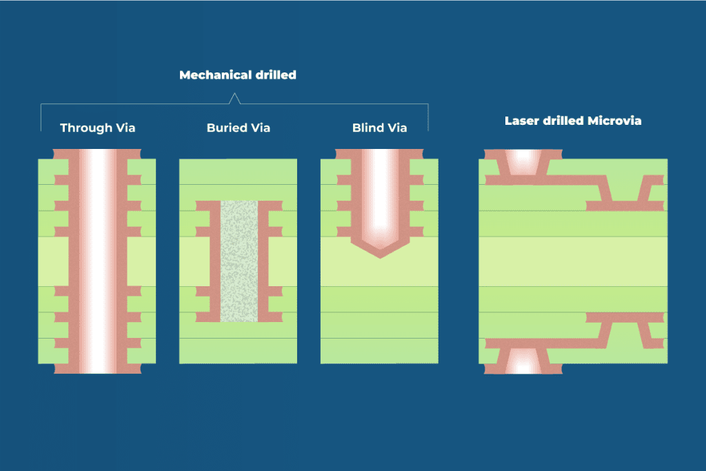
Via holes are used to create electrical or thermal interconnection between layers of a PCB. There are basically 4 types of via holes:
- Through via holes – mechanically drilled holes going through all layers in the stack-up.
- Buried via holes – mechanically drilled holes interconnecting 2 or more inner layers.
- Blind via holes – mechanically drilled holes interconnecting the outer layer with 1 or more inner layers.
- Microvias – laser drilled holes interconnecting 1 layer with the next layer in the stack-up. (It is principally possible to drill microvias mechanically but it is much easier and cost-effective to do with laser.) The most common microvia size is 80-100µm with a depth of 60-100µm. The aspect ratio is the relationship between the dielectric isolating the Cu layers and the diameter of the hole. Most suppliers require an aspect ratio of 0.6 : 1 to 1 : 1 and the most common is 0.8 : 1 (e. Dielectric 80um Laser drill diameter 0.1mm) The new generation of laser drilling machines can drill vias with diameters down to 40-50um and some of them are even able to drill holes simultaneously from both sides of a material which creates the opportunity to laser drill thin dielectrics before the lamination process. This is especially useful during the production of IC Substrate like PCBs.
HDI Stack-up structures and HDI steps
Standard PCBs with PTH (Plated Through Holes) only require 1 lamination, 1 mechanical drilling, 1 hole cleaning, 1 chemical Cu plating, and 1 Galvanic Cu plating. HDI structures may require these steps to be repeated multiple times.
All HDI PCBs start with the construction of the middle inner-layer structures and repeat the lamination, drilling, cleaning, and plating steps until the final stack-up is completed. Let´s show some examples below.
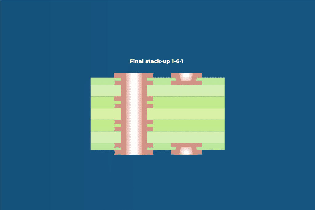
The IPC-2226 Type 1 construction only requires 1 lamination, 1 mechanical drilling, laser drilling from one or both sides, 1-time hole cleaning, 1 chemical Cu plating and 1 Galvanic Cu plating. This is also referred to as a 1-Step HDI.
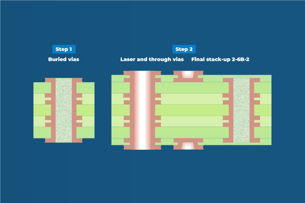
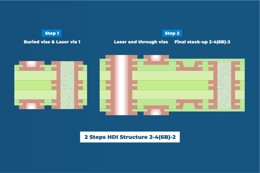
When 1-Step HDI isn’t enough to support the component pitch or general PCB density, additional buried vias can be added to increase the wiring density. The IPC-2226 Type 2 construction requires 2 laminations, 2 mechanical drillings, laser drilling from one or both sides, 2-time hole cleanings, 2 chemical Cu platings, 2 Galvanic Cu platings and 1-time resin filling. This is also referred to as a 2-Step HDI.
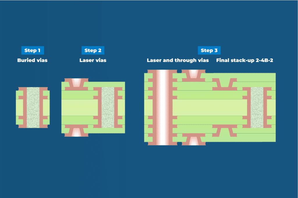
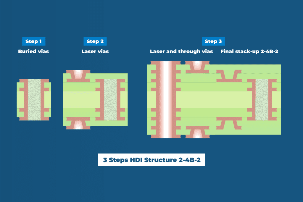
When Type 2 structure isn’t enough to support the component pitch or general PCB density, additional Laser vias and buried vias can be applied. Type 3 structures contain a minimum of 2-step microvias. The IPC-2226 Type 3 construction shown below requires a minimum of 3 laminations, 2 mechanical drillings, 4 times laser drilling, 3-time hole cleanings, 3 chemical Cu platings, 3 Galvanic Cu and platings, and 1-time resin filling. This is also referred to as a 3-Step HDI.
HDI-steps development
BGA pitch has developed from 1,2mm on the very first BGA components to 1,0 and 0,8mm where multilayers containing only through hole via technology was sufficient to create the interconnection and fanouts were achievable with a “dogbone” design. Today most BGA components are only available in pitch 0.5 mm or lower which means that HDI technology with laser-drilled vias are a necessity to make the fanout. In the mobile phone industry, they have even begun to use 0.2 mm pitch BGA components.
This development pushes the limit of the production capability and the equipment used to produce HDI PCBs.
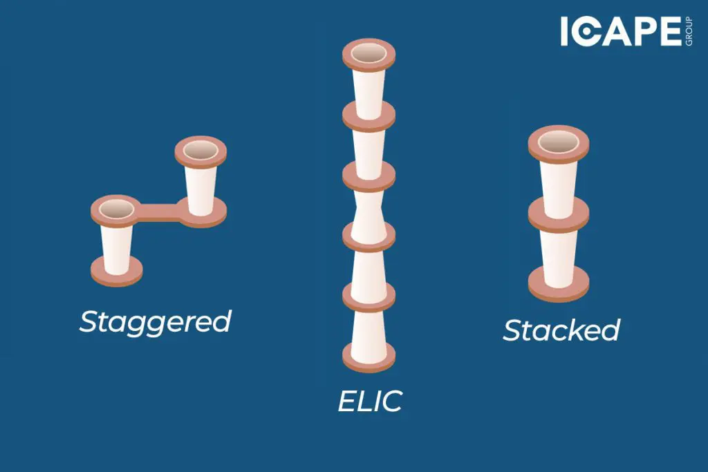
Most complex HDI designs containing BGAs with pitch 0,4-0,5mm can be routed with maximum of 2-4 micro-via steps from each side of the PCB, but some suppliers have mastered 5, 6 or more micro-via steps and the component miniaturization development keeps pushing the limits going in the direction of ELIC (Every Layer Interconnection) also referred to as Any Layer HDI, where stacked vias are deployed through any layer of the stack-up.
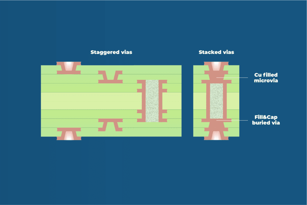
Stacked or Staggered Microvias / Buried vias
The component pitch of the BGA along with its pad size or the design density will dictate when to use stacked or staggered microvias / buried vias or when to use copper-filled vias. Each additional process adds to the overall PCB cost. Firmly executed wire routing and the selection of the optimal HDI stack up and via combination can often contribute to cost reductions. ICAPE would like to support your technology insight with facts and advice:
It is important to choose the best fit via combinations and step combinations to cost-optimize your PCB.
The additional cost of adding a microvia level to a 1-6B-1 structure creating a 2-4(6B)-2 like below, is considerably lower than the cost of a 2-4B-2 structure. Both 1-6B-1 and 2-4(6B)-2 are 2-step HDI constructions but 2-4B-2 is a 3-step HDI.
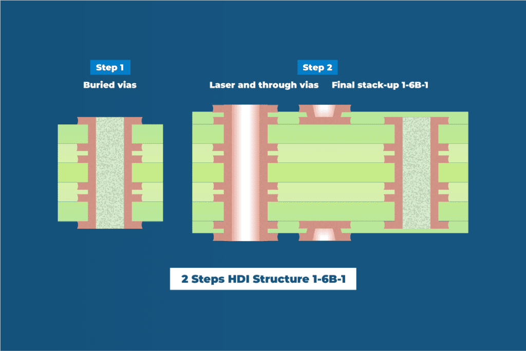
The only extra processes you add going from 1-6B-1 to 2-4(6B)-2 is 2-times laser drilling.
Going from 1-6B-1 to 2-4B-2 requires an extra HDI step with additional 2-times laser drilling, 1 extra lamination 1 extra hole cleaning, 1 extra chem plating, and 1 extra galvanic plating.
Stacked or staggered vias?
Stacked microvias create more space for the high-density wiring and fanout from low-pitch BGAs but it increases the PCB cost. Stacked microvias should only be used when the design doesn´t have sufficient space to use staggered vias. Microvias stacked on buried vias require additional Cu cap plating process for the buried vias and microvias stacked on microvias require additional Cu filling of the inner layer microvias.
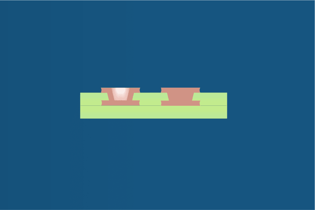
Cu filled Microvias?
Designs with Microvias in BGA pad or similar small soldering pads can benefit from Cu filling since this will eliminate the possibility of air-voids in the solder joints, but the Cu filling increases the PCB cost. Designs without microvias in pad don’t need Cu filling.
Microvia integration on complete design
When you need to use HDI technology with laser-drilled microvias and buried vias due to the wiring density or the component fanout, it makes good sense to replace all mechanical drilled-through vias with laser-drilled microvias and buried vias as this will lower the manufacturing cost and production time.
The laser drilling process is a much faster and cheaper process than mechanical drilling comparing hole to hole cost. The higher price of an HDI PCB compared with standard multilayers is related to the additional processes required for each HDI step. The HDI process step cost is the same whether you only use a few microvias to fan out the BGA wiring, or you replace all through vias with microvias and buried vias. In this instance, replacing all through vias will lower the mechanical drilling process time & cost.
Replacing all through vias on the entire PCB makes sense:
– It will create space for better and tighter wiring leading to higher component population in less space with lower weight.
– It contributes to improved signal integrity, controlled impedance, and reduced electromagnetic interference, by shorter signal paths, reduced transmission lines, and improved GND and VCC reference plane functionality with less hole penetration.
– It eliminates the need for back-drilling on through vias to avoid stub signal reflections.
– HDI PCBs without through vias are more resilient to the thermal stress created by the high temperatures of the soldering processes.
How is mechanical drilled vias and laser drilled produced?
Watch ICAPE PCB Manufacturing Journey episode 5 Drilling.
HDI laser microvias have revolutionized the electronics industry making it possible to pack more functionality into smaller and lighter devices. As technology continues to evolve, microvias will remain at the forefront of PCB design innovation unlocking new possibilities for high-density interconnections and advanced applications. By understanding the types, manufacturing processes, and design considerations associated with microvias, PCB designers can harness their power to create cutting-edge electronic devices for the future.
Sign up to join ICAPE´s next webinar regarding HDI technology where we will share more knowledge and hints to optimize your design and constructions.