
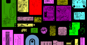
PCB Pooling Techniques : Benefits & Limitations
PCB Pooling Techniques Benefits & Limitations What Is PCB Pooling? PCB pooling is a special manufacturing technique where different customers’ PCB circuit designs are combined
IPC Becomes the Global Electronics Association
IPC Becomes the Global Electronics Association (GEA) The electronics industry is entering a new chapter as IPC officially rebrands itself as the Global Electronics Association
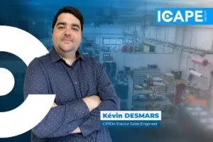
Integrating a new type of conductive ink
Integrating a new type of conductive ink Kevin Desmars : From the Lab to the Factory! Kevin Desmars has always had one foot in fundamental
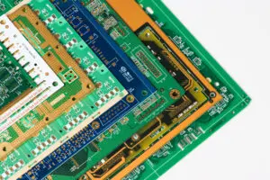
PCB Technologies: The Ultimate Guide – Applications, Advantages, and Industry Insights
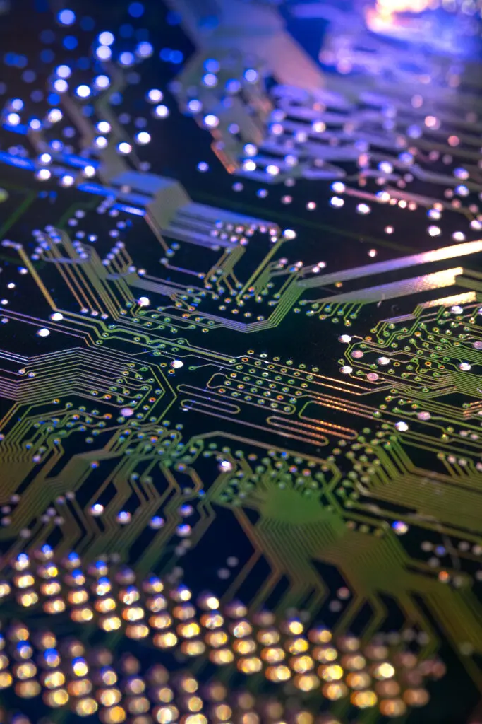
Guide to PCB Technologies Applications, Advantages, and Industry Insights Printed Circuit Boards (PCBs) are the essential foundation of nearly every electronic device—from smartphones and medical

Monitor U.S. Import Tariffs on PCBs & Technical Parts
United States tariff information In April 2025, the United States has implemented new tariffs on Chinese imports, including printed circuit boards (PCBs) and custom-made technical
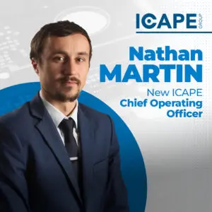
ICAPE Group Appoints Nathan Martin as Chief Operating Officer
ICAPE Group appoints Nathan Martin as Chief Operating Officer ICAPE Group announces the promotion of Nathan Martin to the role of Chief Operating Officer (COO).