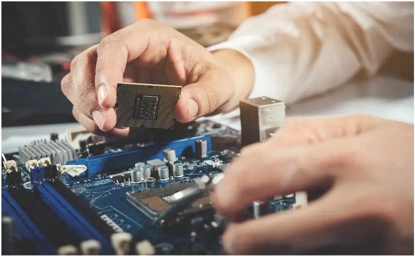
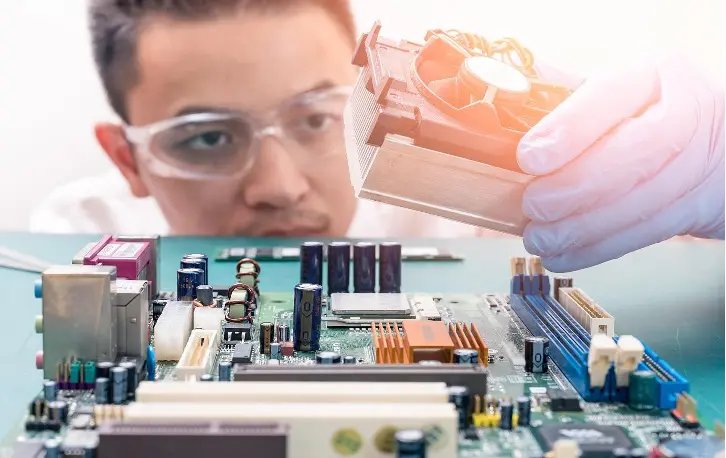
Back Panel PCB
Centralize and interconnect

Back-panel PCBs are a type of printed circuit board that provides a centralized interconnect infrastructure for electronic systems. It simplifies the wiring and interconnect requirements of the complex system, allowing for fast and efficient communication between the individual PCBs.

Product Benefits

The Back-panel PCB serves as a backbone for the electronic system, providing a single point of connection for various electronic modules, daughterboards, and other PCBs. It typically contains many high-speed traces, connectors, and power distribution planes that allow for fast and efficient communication between the active sub-boards. The majority of Back-panel PCBs doesn´t contain any active components.

Ease of assembly

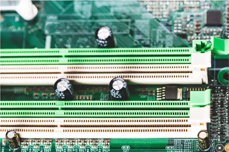
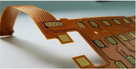
The primarily used components on Back-panels are the connectors used to interconnect the sub-boards. These can be Press-fitted, STM mounted or THT mounted.

Reliability

Back-panel technology provides superior reliability and high-speed connectivity compared with any other interconnection module solutions.

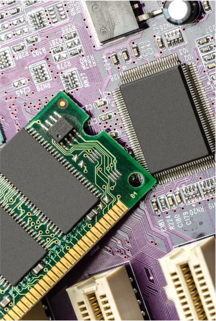
Wide range of materials

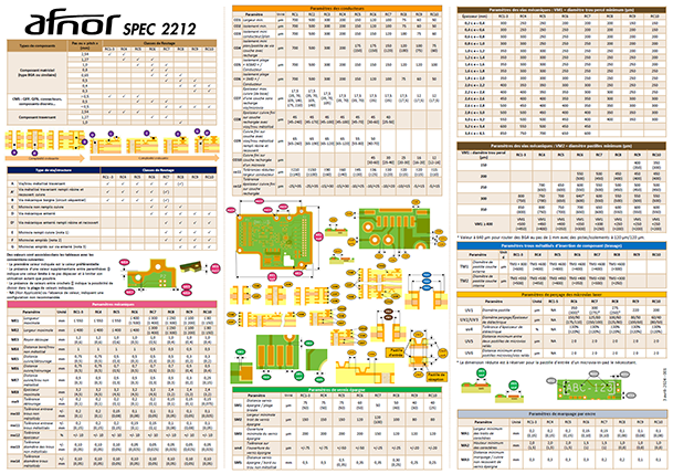
The base material of the back-panel must support high-speed impedance-controlled signal interconnection between various active sub-boards. Most back-panels are built from dedicated high-speed materials with low loss tangent(DF) and the epsilon relative(DK).

What is Back Panel PCB?

Definition

A back-panel PCB is often compared to a personal computer’s motherboard since both contain connections (slots) for sub-boards and allows for communication between all connected boards. The main difference is that the Motherboard used in computer systems contains active component and processors and connections (slots) for expansions boards, where the Back-panel often only contain connections (slots) to interconnect several active boards in larger Server systems.

back panel pcb
back panel specifications

Specifications

Line and space: Back panel PCBs often require impedance-controlled traces which typically mean smaller trace and spacing widths with sizes as small as 0.0025, 0.003 or 0.004 inches (62, 75, 100 microns). Most manufacturers use laser direct imaging (LDI) and vacuum Develop-Etch-Strip (DES) lines to etch the fine patterns.

Vias: Vias are mainly mechanical drilled with min. size approximately 0,3mm. Low possible on request.

Layer count: up to 60 layers

PCB material: We normally recommend using mid or high Tg. material for Back-panel PCBs. Many applications with controlled trace impedances, require special high-speed materials with low signal loss dissipation factor (Df) & low epsilon relative, dielectric constant (εr Dk)

Surface finish: The Back-panel surface treatment depends upon the connector assembly method: Press-fit requires HASL, LF HASL or Immersion Sn. THT and SMT technology requires HASL, LF HASL, OSP, ENIG, Immersion Sn or Immersion Ag.


Active or Passive?

There are two types of back-panel systems: active and passive. Active back panels contain the slots as well as the necessary circuitry to manage and control all the communication between the slots. In contrast, passive back panels contain almost no computing circuitry.

back panel pcb active or passive
back panel pcb size

Thick and rigid with many layers

Back-panels often have a considerable size to support and interconnection of several sub-boards in a rack-system. The extreme number of wires required to interconnect the sub-boards often results in high amount of layers. This makes Back-panels thicker and more Rigid than most PCB. This is a benefit since the PCB needs to be stiff enough to support the insertion force plugging the sub-boards into the back-panel connectors. Rigid-Multilayers are the most common technology used to develop back panels, but Flex-Rigid can also be developed in the case of special cabinet solution.

Do you need Back-Panel PCB's?

Back-panels are the backbone for any larger computing or server system. It offers a firm and robust mechanical platform allow low-ohm high-speed interconnection between all the sub-boards the complex electronic system.

Technical Data

Back Panels

Back Panels FeatureICAPE Group back panel technical specification
Layer countUp to 60 layers.
MaterialsHigh TG, High-Speed and low loss materials
Base Copper ThicknessFrom 1/3 Oz base to 2 Oz finished thickness
Minimum track & spacing0.062mm / 0.075mm
Surface finishes availableHASL, LF HASL, OSP, ENIG, Immersion Tin, Immersion Silver.
Minimum mechanical drill0,3mm (Advanced 0.2mm)
PCB thickness1,6mm – 6.0mm. (Advanced 8mm)
Maximum dimensions590x680mm.

Close to you, you best contact

Learn more about Back-Panel PCBs

Webinars

ICAPE Group invites you to our free technical webinars to enhance your knowledge of PCB technologies, technical part commodities, design, and materials.
high voltage power

Industries

Discover how Back-Panel PCB impacts several different industries and multiple fields.

flex pcb

Technologies

Learn about the different technologies in the PCB industry and find which one suits your needs best. 

Any questions?

There is an ICAPE Group team close to you and your business. All around the world, our business units are staffed with native experts available to answer all your questions.

 Contact us today!