
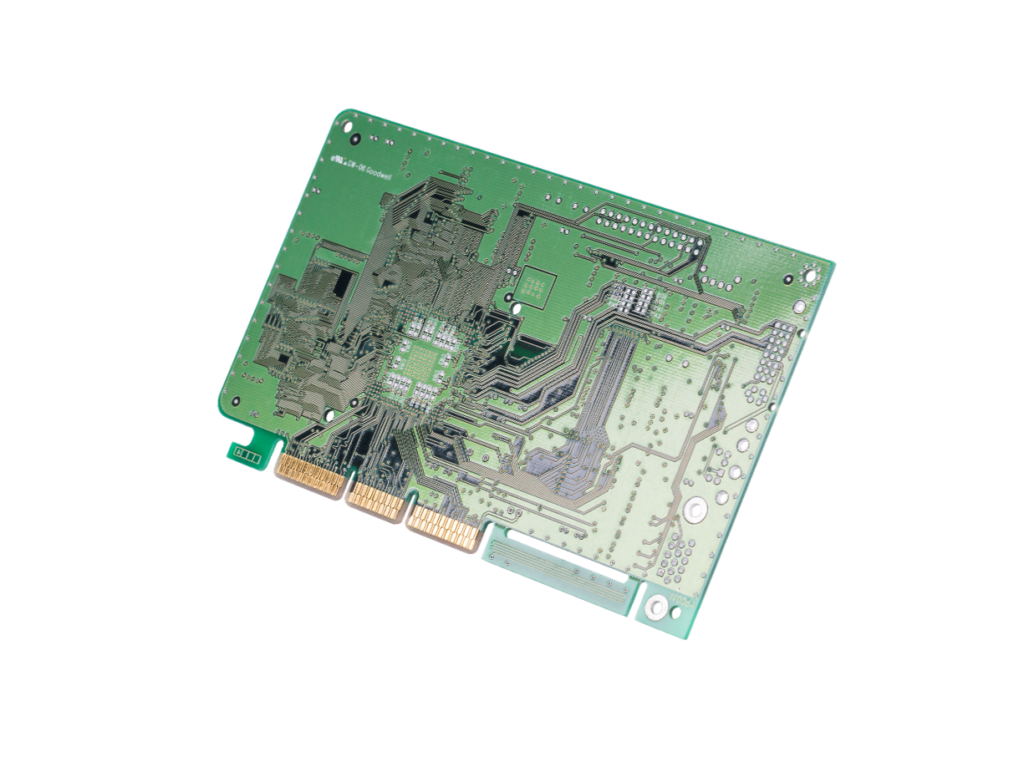
PCB Density
Density is the ratio of traces, holes, and pads by area unit (mm², inch², etc…) When there are only a few traces, density is not an issue. But modern density requires modern solutions and every day, the customers and the factories are asking for more compact and more complex designs mainly due to the component technologies. The higher the density, the more complex the PCB is.
The Challenges for Production
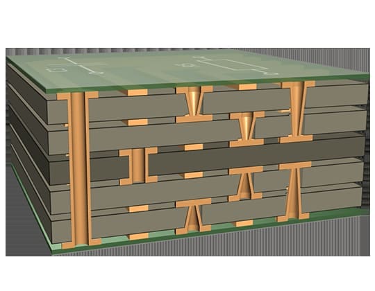
With the advancement and the miniaturization of electronics, the demand for HDI PCBs has increased drastically but increasing density on a printed circuit board is a challenge from design to production. The spaces between the traces are down to 65µm. HDI PCBs are made with at least 4 layers, connected to each other by holes and vias to make ultra-complex design rules and production processes.
If the design is challenging for the engineers with their software, one of the main problems in production is to ensure the reliability of the plated holes. The main problem comes from the vias and holes and the plating process. To assume a good hole plating integrity, the aspect ratio is limited to 1: 0.8 for blind vias, advanced value is 1:1. Standard pre-pregs also contain fiberglass which is too thick for laser drilling. The glass contained in the pre-preg changes the laser direction and creates a mediocre or wrong shape quality of the laser via holes.
Main Capabilities
| HDI | Capabilities |
|---|---|
| Number of layers MIN & MAX | 4-24L |
| HDI Builds 1+N+1, 2+N+2 | 3+N+3 and anylayer |
| Materials FR4, ..., ETC. | See table |
| Copper Weight MIN & MAX | 0.5oz~6oz |
| Minimum track & gap MM | 65/65μm |
| PCB Thickness MIN & MAX | 0.4-2.8mm |
| Dimension MAX | 0.457*508mm |
| Surface Finishes OSEP, ENIG, ETC. | HASL, HASL LF, ENIG, immersion tin, OSP, immersion silver, electroplating hard gold/soft gold, gold finger, selective OSP, ENEPIG |
| Mechanical Drill MIN | 0.15mm |
| Laser Drill MIN | 0.076mm |
Enhancing HDI PCB Design and Reliability
Any questions?
There is an ICAPE Group team close to you and your business. All around the world, our business units are staffed with native experts available to answer all your questions. Contact us today!