
87% Say Sustainability Will Dominate in 5 Years
87% say sustainability will dominate in 5 years What does that mean for product Roadmaps? The electronics industry powers nearly every aspect of modern life,
PCB Technical Guides & Resources
Technical guides and resources PCB and Tech Parts explained Welcome to ICAPE Group’s comprehensive guide hub – your reference point for everything related to Printed
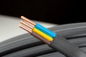
Electronic Cables: Types, Materials, Uses, and Technical Specifications
Guide to Electronic Cables Types, Materials, Uses, and Technical Specifications From powering up your device to transmitting data at lightning speed, electronic and optical cables
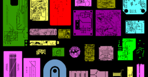
PCB Pooling Techniques : Benefits & Limitations
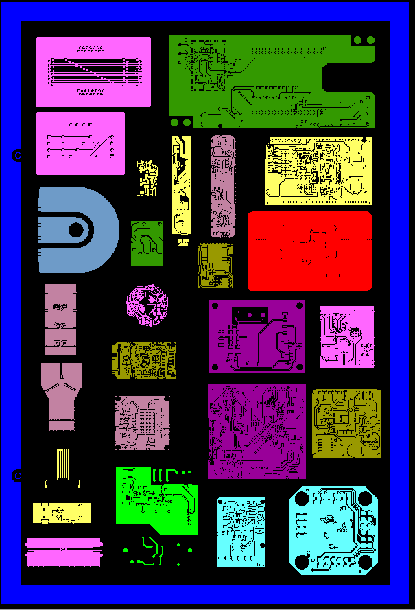
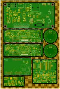
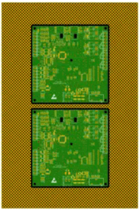
PCB Pooling Techniques Benefits & Limitations What Is PCB Pooling? PCB pooling is a special manufacturing technique where different customers’ PCB circuit designs are combined
IPC Becomes the Global Electronics Association
IPC Becomes the Global Electronics Association (GEA) The electronics industry is entering a new chapter as IPC officially rebrands itself as the Global Electronics Association
Integrating a new type of conductive ink
Integrating a new type of conductive ink Kevin Desmars : From the Lab to the Factory! Kevin Desmars has always had one foot in fundamental