The inner layer imaging is a very technical step of the process which happens in a clean and yellow room. Why ? Because the dry film is UV sensitive and to avoid any shorts and opens on the inner layer, a level between 3000 and 4000 dust particles per cubic meters must be reached.
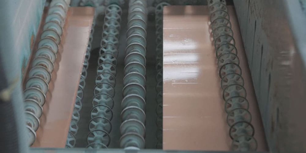
1 - CLEANING
The cleanroom uses overpressure to protect and remove any dust coming from outside of the cleanroom. Before entering the cleanroom, the panels are cleaned. Depending on the thickness of the inner layers, the processes are different. For layers thinner than 500 micrometers, the chemical process is used. For thicker layers, the mechanical process is preferred.
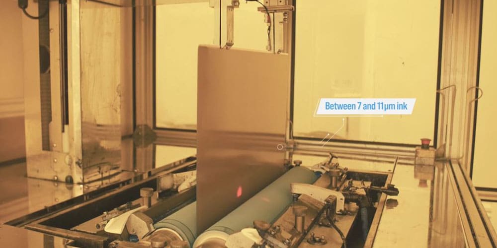
2 - ENDUCTION
When panels arrive in the cleanroom, they are heated, then the photoresist film or the ink ( beteween 7 and 11 µm) is automatically applied onto the panel.
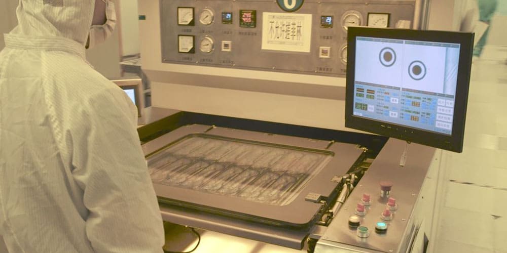
3 - REGISTRATION AND INSOLATION
The boards are registered at +/- 15 to 30 micrometers with 2 or 4 CCD Cameras. A vacuum is created, then a blast of UV light is applied with an average of 1 to 20 seconds depending on the process: this is the insolation. The boards are polymerized and ready to be developed.
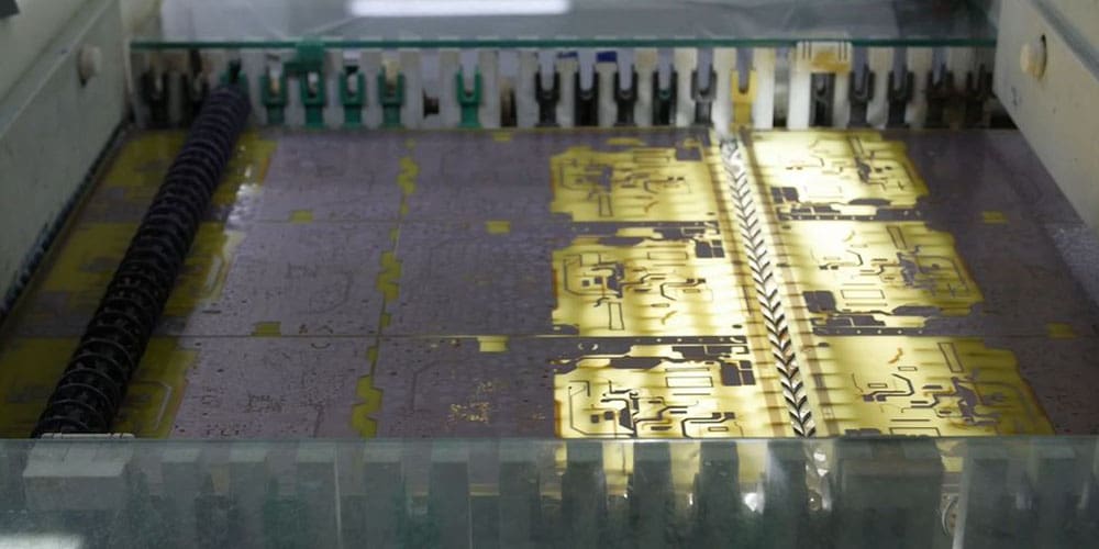
4 - DEVELOPING AND ETCHING
For the development phase, the board is washed with an alkaline solution which removes the photoresist left unhardened. From there, we can see the inner layer image for the first time. Etching is the critical step in layer imaging. The unprotected copper is removed and defines the pattern. After stripping the ink, the photoresist film is now completely removed.
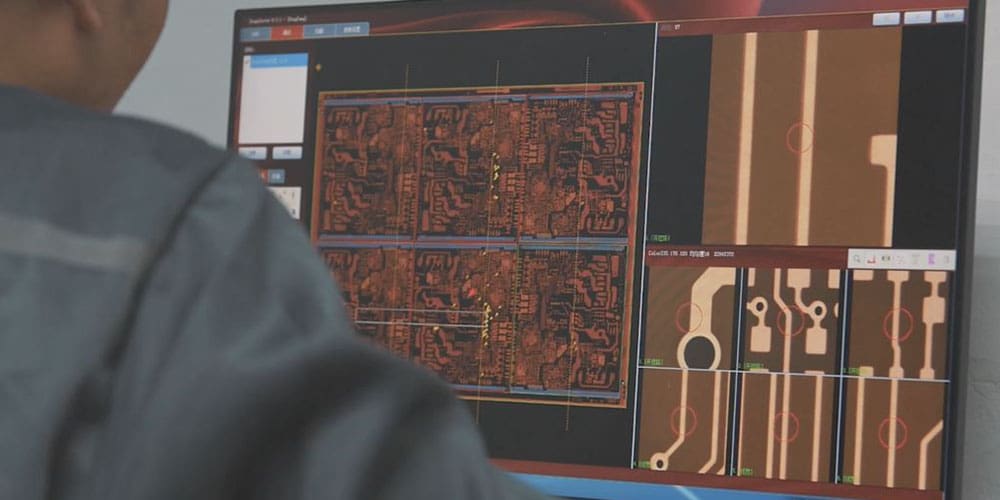
5 - AUTOMATIC OPTICAL INSPECTION (AOI)
After the Multilayer lamination, it is impossible to correct errors occurring on the inner layers. The Automatic Optical Inspection will confirm a total absence of defects. The original design from the GERBER file serves as a model. If the machine detects any inconsistencies, a technician will assess the problem.
Other steps
Welcome
To ensure compliance with European data protection regulations, please verify you are in Europe.