The solder mask has two interests. The first is to avoid the oxidation of copper and the second is to have perfect insulation between two traces of copper during the assembly process. There are different types of PCB soldermask, such as Epoxy Liquid, Liquid Photoimageable (LPI), or Dry Film. Let’s dive into it!
1 - COATING
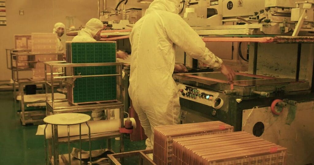
There are different ways to apply the solder mask to a PCB: curtain, screen printing or electrospray deposition coating according to IPC standards. Before any solder mask application, the boards must be cleaned with a mechanical or chemical preparation in an over-pressurized cleanroom to prevent dust from entering from the outside.
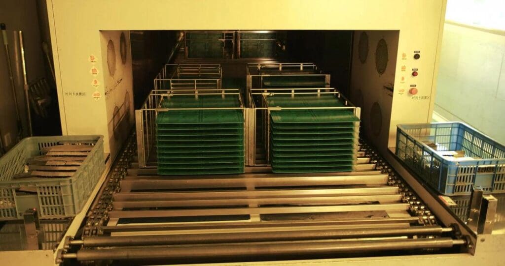
2 - PRE-CURING
Once the panel is totally covered, it must be pre-cured. This step is essential and removes all the solvent from the ink. Without this step, registration will not be done properly.
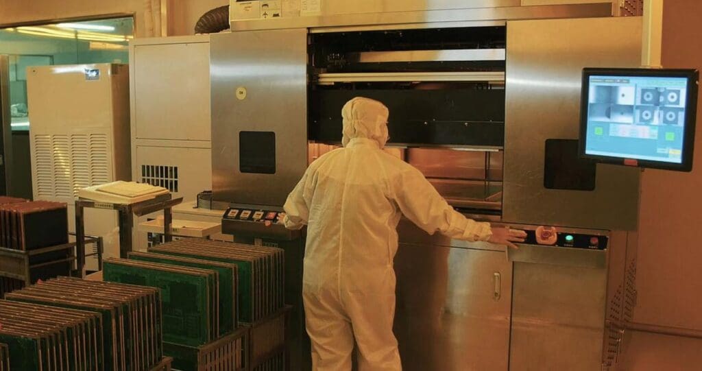
3 -REGISTRATION/INSOLATION
For the soldermask, the insolation can be done with the registration with 8 CCD cameras and the artwork. The boards receive a blast of LED light for a few seconds to harden the soldermask where the artwork is clear. The insolation can also be done by LDI, Laser Direct Imaging. This time, no artwork is necessary because the machine directly insoles the selected locations with light beams and hardens the targeted location.
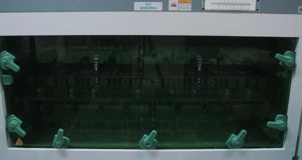
4 - DEVELOPING
The portions not protected and not hardened by the insolation are washed away. Here, in our example, the soldermask around the mechanical through-hole is removed.
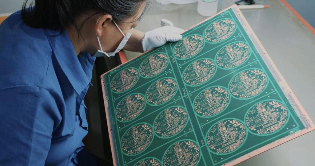
5 - CONTROL AND CURING
After the developing phase, all the boards are controlled. Indeed, inspection is needed to check if there are any defective images, traces of ink on the pads or through the holes. Finally, the boards are exposed to a high temperature for one hour to cure the soldermask.
Other steps
Welcome
To ensure compliance with European data protection regulations, please verify you are in Europe.