

ICAPE Group expands its custom electronic parts portfolio with PTC Heaters
ICAPE Group expands its custom electronic parts portfolio with PTC Heaters Smart, efficient thermal management solutions ICAPE Group continues to broaden its range of high-performance
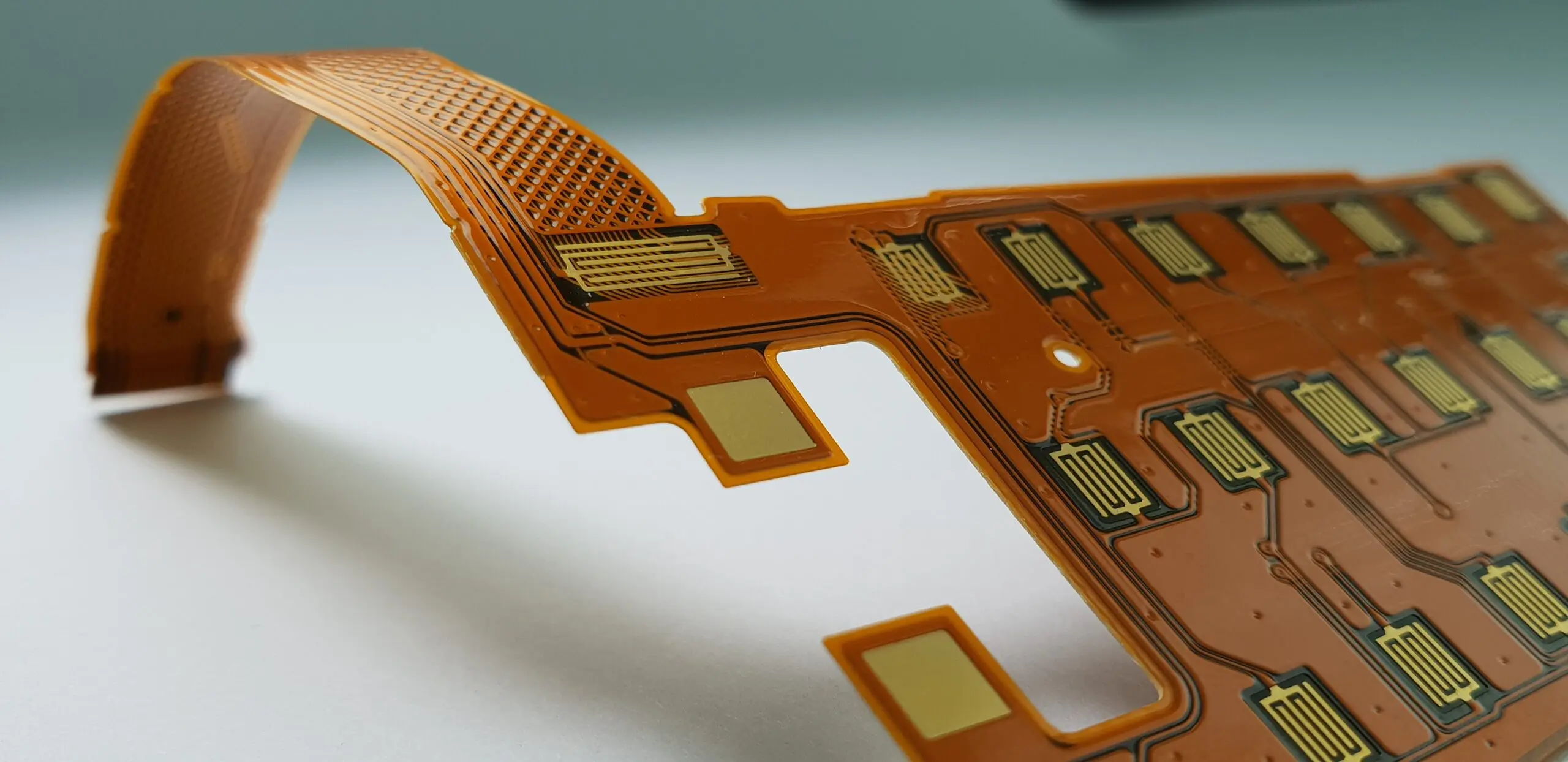
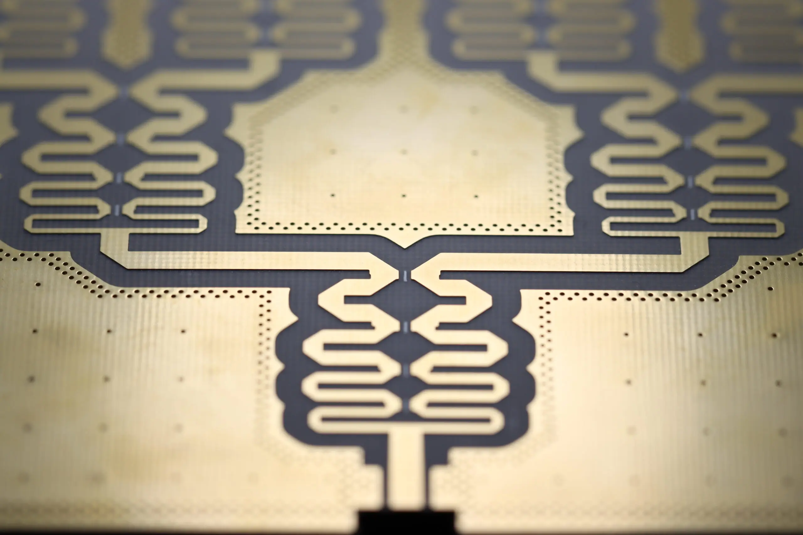
The C-FLEX Jumper arrives in ICAPE Group’s product range !
The C-FLEX Jumper arrives in ICAPE Group’s product range ! Compact reliable and European-made flexible circuit ICAPE Group expands its high-reliability interconnection solutions with the launch of

ICAPE Group’s Global CSR Achievements
ICAPE Group’s Global CSR Achievements Building a responsible and sustainable future At ICAPE Group, we see sustainability as the foundation of long-term performance. Every decision,

87% Say Sustainability Will Dominate in 5 Years
87% say sustainability will dominate in 5 years What does that mean for product Roadmaps? The electronics industry powers nearly every aspect of modern life,

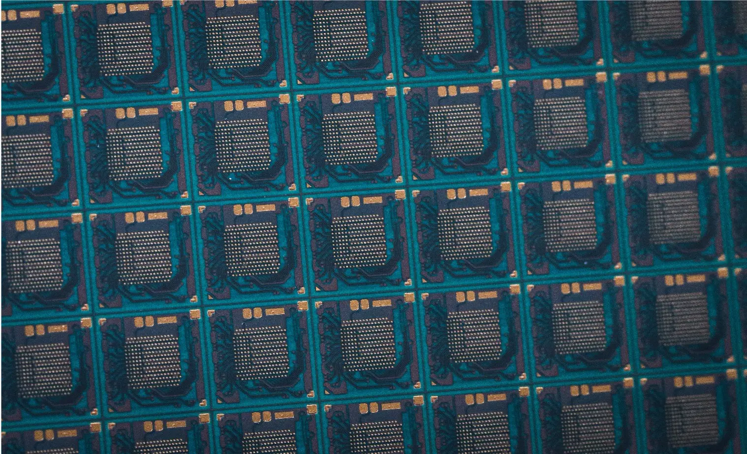
PCB Technical Guides & Resources
Technical guides and resources PCB and Tech Parts explained Welcome to ICAPE Group’s comprehensive guide hub – your reference point for everything related to Printed
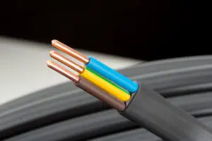
Electronic Cables: Types, Materials, Uses, and Technical Specifications
Guide to Electronic Cables Types, Materials, Uses, and Technical Specifications From powering up your device to transmitting data at lightning speed, electronic and optical cables