

The Outer Layer Imaging is similar to the Inner Layer Imaging, but much more complex with the holes and the surface roughness. Let’s see how this spectacular step of the PCB manufacturing process is done!
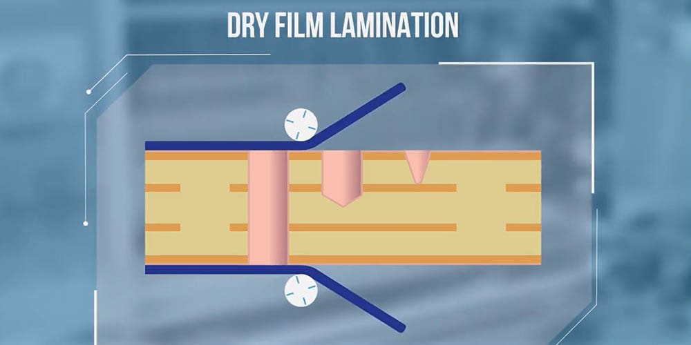
The surface is prepared: boards thinner than 500 micrometers undergo a chemical cleaning process, while thicker boards undergo a mechanical cleaning process using abrasive brushes. The boards are heated for better adhesion of the photoresist film. Then, the boards are coated with an automatic lamination on X and Y. The edge is cut directly by the machine.
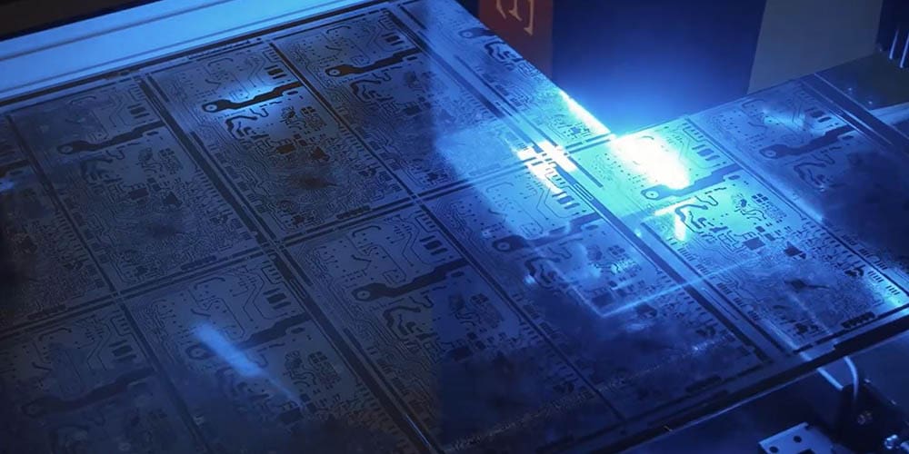
For semi-automatic insolation, the artwork is checked again before being added to the machine. Registration is optically done between the holes and the targets with 2 or 4 CCD cameras. Once the panel meets the quality criteria, a vacuum is applied, then the board receives a blast of UV light between 1 and 20 seconds to polymerize the photoresist, creating an image of the circuit pattern.
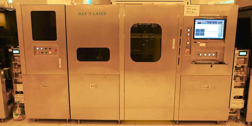
For high-end products and high-density materials, Laser Direct Imaging is used. This machine is fully automatic, so loading, registration with 4 CCD cameras and transferring the layer image is done in seconds. LDI is also an important factor when close tolerances and tight registration are involved, such as 50 micrometers or less.
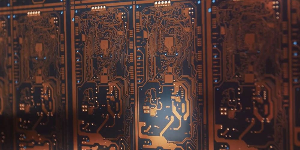
Once the insolation is finished, the protection on the dry film is removed. The areas not exposed to UV Light or Laser are unhardened and will be dissolved in the developing sodium bath leading the boards to this beautiful blue color. The outer layer image is now printed, ready to receive electrolytic copper.
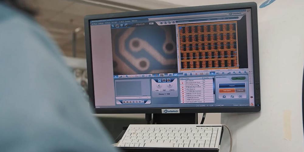
The Automatic Optical Inspection of the outer layers will confirm the total absence of defects, whether electrical opens or shorts. As with the Inner Layer, the original design from the GERBER file serves as a model for the optical camera. If the machine finds an inconsistency, a technician will assess the issue.
To ensure compliance with European data protection regulations, please verify you are in Europe.