
HDI PCB: Smaller, Faster, and Denser
for Modern Technologies
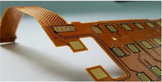
High-Density Interconnect (HDI) printed circuit boards have become one of the most important enablers of modern electronics. By combining microvias, fine lines and spaces, and sequential lamination techniques, HDI PCBs make it possible to fit more functionality into smaller, lighter products without compromising electrical performance. They are the foundation behind the compact smartphones we carry, the high-speed networking systems that connect us, and the advanced medical and automotive devices that demand both reliability and miniaturization.
Product Benefits
At ICAPE Group, we specialize in the design, prototyping, and large-scale manufacturing of HDI PCBs. Our global network of audited factories and engineering experts allows us to deliver boards that not only meet the tightest design rules but also remain cost-effective and scalable.

Better Signal Integrity
HDI helps in placing the components closer to each other which cuts down the signal path length. It removes via stubs, reduces reflections of signals, and thus improves signal quality.

High Reliability
Laser-drilled microvias have less chance of manufacturing mistakes and interconnecting defects during PCB production compared with conventional via PTHs (plated through holes). The microvias are also less affected by CTE (Coefficient of Thermal Expansion) during the assembly process.

Cost-Effective
Although the square meter price is higher for HDI PCBs, the superior signal integrity, higher reliability, and space, weight, and layer savings make HDI PCBs a cost-effective quality solution.
Key Facts
- HDI = compact, high-density printed circuit boards
- Core technologies: microvias, fine lines, sequential lamination
- Applications: smartphones, networking, medical, automotive
- Benefits: more functions in less space
What is an HDI PCB?
An HDI PCB is defined by its exceptionally high wiring density compared to conventional multilayer boards. This is achieved through the use of laser-drilled microvias, with diameters typically below 150 microns, and conductor widths and spacings that can be reduced to 75 microns or less. The result is a circuit board that can accommodate fine-pitch components such as BGAs and CSPs while maintaining signal integrity at high frequencies.
HDI boards are usually built with sequential lamination processes, where thin dielectric layers are stacked and laminated one by one. Blind and buried vias are introduced to create interconnections only where needed, saving valuable routing space and reducing parasitic effects. In essence, HDI technology allows engineers to pack more performance into less physical volume, which is why it has become indispensable in mobile, computing, and communication devices.
Advantages of HDI Technology
The key advantage of HDI PCBs lies in their ability to combine miniaturization with improved electrical characteristics. By using microvias instead of traditional through-holes, designers reduce signal path lengths, which minimizes delay and crosstalk in high-speed circuits. Controlled impedance can be achieved more easily with carefully designed stackups, which is critical for DDR4, 5G, and RF applications.
Another often overlooked benefit is reliability: microvias, due to their lower aspect ratios, generally withstand thermal cycling better than deep drilled holes. At the same time, the use of buried and blind vias allows engineers to reduce the overall number of layers, saving space and weight. For industries like aerospace or wearable devices, these gains in efficiency and reliability are essential.
 Improved signal integrity
Lower crosstalk and delay
Miniaturization (fewer layers, lighter)
High reliability (thermal cycling, microvias)
Ideal for 5G, RF, DDR4/5, aerospace, wearables
Feature
Via type
Trace width / spacing
Layers needed
Applications
Standard PCB
Through-hole
100–150 μm
Higher (e.g. 12)
General electronics
HDI PCB
Microvia (≤150 μm)
50–75 μm
Fewer (e.g. 8 with HDI)
Mobile, RF, high-speed
Technical Data
HDI
| HDI Feature | ICAPE Group HDI Technical Specification |
|---|---|
| Layer count | Up to 24 layers standard. Advanced 36 layers. |
| Technology highlights | High Density Interconnection PCB with laser blind holes. POFV, up to 4 sequential laminations (N+4). Advanced N+6, ELIC 14 Layers (X-Via). |
| Materials | FR4 raw material with high TG, low CTE, halogen-free, Hi-Speed and low loss specifications. |
| Base copper thickness | 1/3 Oz to 2 Oz |
| Minimum track & spacing | 0.075mm / 0.075mm – Advanced 0.075mm / 0.05mm |
| Surface finishes available | OSP, ENIG, ENEPIG, Soft-Gold, Gold fingers, Immersion Tin, Immersion Silver. Advanced selective OSP / ENIG. |
| Minimum laser drill | 0.10mm. Advanced 0.05mm. |
| Minimum mechanical drill | 0.125mm. Advanced 0.1mm. |
| PCB thickness | 0.40mm – 3.2mm. Advanced 5mm. |
| Maximum dimensions | 525×680mm. Advanced: 980×360mm. |
Types of HDI Structures
Not all HDI boards are built the same way. Industry standards classify them into several types depending on the number and arrangement of microvia layers. Type I designs include a single build-up layer of microvias, either on one or both sides of the core. Type II adds buried vias into the mix, allowing more flexible interconnections without increasing layer count excessively. Type III, often used in advanced applications, involves multiple stacked microvia layers, which greatly increases routing density but also raises manufacturing complexity.
At the very high end, Any-Layer HDI — sometimes referred to as Ultra-HDI — allows interconnection between any two layers in the stack. With line widths below 50 microns and microvias smaller than 75 microns, this technology enables the most compact layouts in smartphones and RF modules, where every square millimeter of space matters.
- Type I (single build-up)
- Type II (buried vias included)
- Type III (multiple stacked microvias)
- Any-Layer HDI (connections possible between any layers, ultra-compact).
Comparison of HDI Types
| HDI Type | Structure | Complexity | Applications |
|---|---|---|---|
| Type I | Single microvia layer | Low | Consumer, entry-level HDI |
| Type II | Microvia + buried vias | Medium | Networking, automotive |
| Type III | Stacked microvias (multi-layer) | High | High-speed, telecom, servers |
| Any-Layer HDI | Microvias between all layers | Very High | Smartphones, RF modules, 5G |
Manufacturing Processes
Compared to classical fixed resistance heaters, printed PTC heaters deliver clear advantages:
Producing an HDI PCB requires a set of advanced processes that go beyond standard multilayer fabrication. Microvias are created using laser drilling, which ensures the precision required at such small diameters. Sequential build-up lamination is then performed to add dielectric layers one at a time, embedding blind and buried vias as needed. When via-in-pad structures are required — a common necessity under fine-pitch BGAs — the vias must be copper-filled and planarized to guarantee both mechanical strength and solderability.
Surface finishing also plays an important role. ENIG is widely chosen for its durability and solder joint reliability, while OSP and ImmAg offer cost-effective alternatives depending on assembly requirements. Finally, stringent inspection processes such as AOI, X-ray via analysis, and impedance testing ensure that the complexity of HDI does not compromise product reliability.
Manufacturing HDI Key Steps
- Laser drilling → microvias ≤150 μm
- Sequential lamination → adds layers one by one
- Via-in-pad → copper-filled & planarized for BGAs
- Surface finishing → ENIG / OSP / ImmAg
- Inspection → AOI, X-ray, impedance test
Design for Manufacturing (DFM) Guidelines
Because of their complexity, HDI PCBs require careful attention to DFM rules from the earliest design stages. Microvia diameters typically range from 0.10 to 0.15 mm, but exact limits vary depending on factory capabilities. Trace widths and spacings of 75 microns are common, though Ultra-HDI designs push this further down to 50 microns. When via-in-pad is used, copper filling is not optional — it is the only way to achieve reliable solder joints under fine-pitch packages.
Engineers should also define impedance requirements clearly in the stackup documentation, usually with a tolerance of ±10 ohms for high-speed designs. To avoid delays, all design files — Gerbers or ODB++, drill maps, stackup drawings, and netlists — must be provided together. At ICAPE, we supply a downloadable DFM checklist to help customers validate these requirements before production, reducing iterations and ensuring first-pass success.
Technical Data
HDI
| HDI Feature | ICAPE Group HDI Technical Specification |
|---|---|
| Layer count | Up to 24 layers standard. Advanced 36 layers. |
| Technology highlights | High Density Interconnection PCB with laser blind holes. POFV, up to 4 sequential laminations (N+4). Advanced N+6, ELIC 14 Layers (X-Via). |
| Materials | FR4 raw material with high TG, low CTE, halogen-free, Hi-Speed and low loss specifications. |
| Base copper thickness | 1/3 Oz to 2 Oz |
| Minimum track & spacing | 0.075mm / 0.075mm – Advanced 0.075mm / 0.05mm |
| Surface finishes available | OSP, ENIG, ENEPIG, Soft-Gold, Gold fingers, Immersion Tin, Immersion Silver. Advanced selective OSP / ENIG. |
| Minimum laser drill | 0.10mm. Advanced 0.05mm. |
| Minimum mechanical drill | 0.125mm. Advanced 0.1mm. |
| PCB thickness | 0.40mm – 3.2mm. Advanced 5mm. |
| Maximum dimensions | 525×680mm. Advanced: 980×360mm. |
Cost and Lead Time
Compared to conventional multilayers, HDI boards are more costly to produce due to additional drilling, plating, and lamination steps. However, they often reduce the total layer count, offsetting part of this cost. For example, a 12-layer standard PCB can sometimes be replaced by an 8-layer HDI design with equivalent routing capacity.
Lead times depend on complexity: prototypes can be delivered within 7–15 business days, while mass production typically requires 15–35 days. The main cost drivers include the number of build-up cycles, the use of stacked microvias, and whether via-in-pad is specified. With ICAPE’s global sourcing network, customers benefit from optimized pricing while maintaining strict quality standards.
Cost Factors
• More lamination cycles = higher cost
• Stacked microvias = more complexity
• Via-in-pad = extra plating, higher price
• Reduced layer count offsets cost
• Prototypes: 7–15 days
• Mass production: 15–35 days
Why Choose ICAPE Group
ICAPE Group has been a leader in PCB sourcing and manufacturing services for over 20 years. Our network of carefully audited partner factories includes multiple sites specialized in HDI production, capable of meeting requirements from single-stack microvia builds to complex any-layer HDI structures.
What sets us apart is our combination of engineering support and supply chain flexibility. We provide DFM analysis, stackup optimization, and pre-production checks to ensure that your design is manufacturable from the very beginning. Every board undergoes AOI, X-ray inspection, and electrical testing before delivery. Whether you need a rapid prototype, a mid-sized production run, or high-volume manufacturing, ICAPE offers a scalable solution backed by local service teams in more than 20 countries.
By choosing ICAPE Group, you secure not only an HDI PCB supplier but also a long-term partner committed to reliability, cost efficiency, and global support.
ICAPE Group’s Benefits
- 20+ years of PCB expertise
- Audited global factory network
- Support from design to production
- DFM + stackup optimization
- Full testing: AOI, X-ray, impedance
- Local teams in 20+ countries
An HDI PCB (High-Density Interconnect PCB) is a printed circuit board that uses fine lines, microvias, and sequential lamination to achieve much higher wiring density than standard multilayer PCBs. This enables smaller, lighter, and faster electronic products.
A microvia is a very small via, usually laser-drilled, with a diameter of 0.10–0.15 mm (≤150 μm). Unlike traditional vias, microvias typically connect only one layer to the next, reducing space consumption and improving signal integrity.
- Through-hole vias: connect all layers, drilled mechanically.
- Blind vias: connect an outer layer to one or more inner layers.
- Buried vias: connect only inner layers, invisible from the surface.
HDI PCBs often combine all three to save space and increase density.
Via-in-pad is a technique where vias are placed directly under component pads (e.g., BGAs). In HDI, these vias are filled with copper and planarized to create a flat, solderable surface. This is essential for fine-pitch packages and high-speed performance.
- HDI PCBs use microvias, finer lines (<75 μm), and sequential lamination, while standard PCBs rely on through-holes and thicker traces.
- HDI boards achieve higher routing density, allowing fewer layers overall.
- Standard PCBs are cheaper and easier to fabricate but cannot support today’s miniaturized, high-speed electronics.
Ultra-HDI, also called Any-Layer Interconnect (ALIVH), is the most advanced form of HDI. It allows vias between any two layers, often with line widths below 50 μm and microvias below 75 μm. This is commonly used in smartphones, 5G modules, and high-frequency RF devices.
- Consumer electronics: smartphones, tablets, wearables
- Telecom & networking: 5G, servers, routers, base stations
- Medical: imaging, diagnostic equipment, implants
- Automotive: ADAS, infotainment, EV power modules
- Aerospace & defense: lightweight, high-reliability systems
- Miniaturization (more components in less space)
- Shorter signal paths (better electrical performance)
- Lower crosstalk and delay
- Higher reliability (microvias withstand stress better)
- Reduced total layer count compared to standard multilayers
- Precise laser drilling for microvias
- Copper filling of via-in-pad structures
- Multiple sequential lamination cycles
- Advanced inspection (X-ray, AOI, impedance testing)
These processes require specialized factories and tight process control.
Microvias are typically designed with an aspect ratio below 1:1. For example, a 100 μm hole depth should have a maximum 100 μm diameter. Lower aspect ratios improve plating quality and reliability.
HDI PCBs often use high-performance laminates such as FR-4 high-Tg, polyimide, or low-loss materials (e.g., Megtron, Rogers) depending on application. Material choice impacts impedance control, thermal stability, and cost.
- ENIG (Electroless Nickel Immersion Gold): most common, reliable, flat
- OSP (Organic Solderability Preservative): cost-effective
- Immersion Silver / ImmAg: good for fine-pitch soldering
- ENEPIG: excellent for wire bonding
Choice depends on assembly method, shelf life, and reliability requirements.
By using blind/buried vias and microvias, routing density increases, so fewer overall layers are needed. For instance, a 12-layer standard PCB might be replaced by an 8-layer HDI PCB with equivalent performance.
HDI PCBs are more expensive per unit area due to additional lamination cycles, laser drilling, and copper filling. However, cost can be offset if the design reduces total layer count. Final pricing depends on:
- Layer count & stackup complexity
- Microvia type (stacked vs staggered)
- Via-in-pad usage
- Material selection (FR-4 vs high-speed laminate)
- Production volume
- Prototypes: 7–15 business days
- Mass production: 15–35 business days
Lead time increases with complexity (number of build-ups, stacked vias, surface finish).
When properly manufactured, HDI PCBs are highly reliable. Copper-filled microvias provide strong mechanical integrity, and lower aspect ratios improve thermal cycling performance. The main risks come from poor plating or misaligned stacked vias, which is why quality control (X-ray, cross-sectioning) is critical.
To avoid production delays, you should provide:
- Gerber or ODB++ files
- Drill map and via specifications
- Stackup drawing with impedance requirements
- Netlist for electrical testing
- Assembly drawings (if via-in-pad or special requirements)
All ICAPE HDI PCBs undergo:
- Automated Optical Inspection (AOI)
- X-ray via analysis
- Electrical testing (100%)
- Impedance control verification
- Cross-section analysis upon request
Do you need HDI PCBs?
HDI is a necessity when the component pitch requires it, or the board size demands it. When properly designed, HDI PCBs are smaller, thinner, and weigh less (board downsizing trend). HDI has a myriad of constructions and variables that all affect density. To understand how blind vias, skip vias, staggered vias, stacked vias, and buried vias contribute to density, you must do a “routing test” and play with all these different stack-ups and constructions. By measuring the metrics (inches/square inch and pins/square inch), you can create a table that relates these density measures to the corresponding construction.
HDI PCB design techniques are used when considering the need to mount extreme component density on a limited board size. The component density determines the number of connections per square inch of the board. If the connections of all the parts and test points divided by the size of the board are less than 120 — 130 pins per square inch, there is no need to be using HDI, unless the use of specific dense BGA requires HDI to facilitate all connections. HDI technology has revolutionized the electronics industry and is used in most electronic gadgets you know. The demand for Printed Circuit Board using HDI technology looks promising for many various industries.
Learn more about HDI

Webinars on Demand - HDI
If you’ve missed a webinar, we now offer various webinars on demand, available upon request!
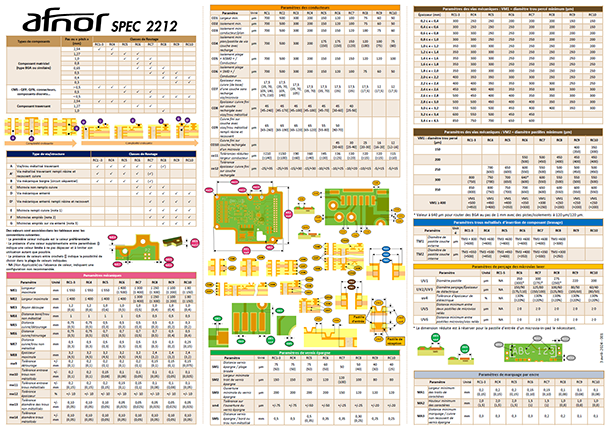
AFNOR PCB Design Guide
AFNOR SPEC 2212 is a benchmark specification developed to address the growing need for robust, sustainable, and forward-thinking solutions in PCB design
Technologies
Learn about the different technologies in the PCB industry and find which one suits your needs best.
Any questions?
There is an ICAPE Group team close to you and your business. All around the world, our business units are staffed with native experts available to answer all your questions.
Contact us today!