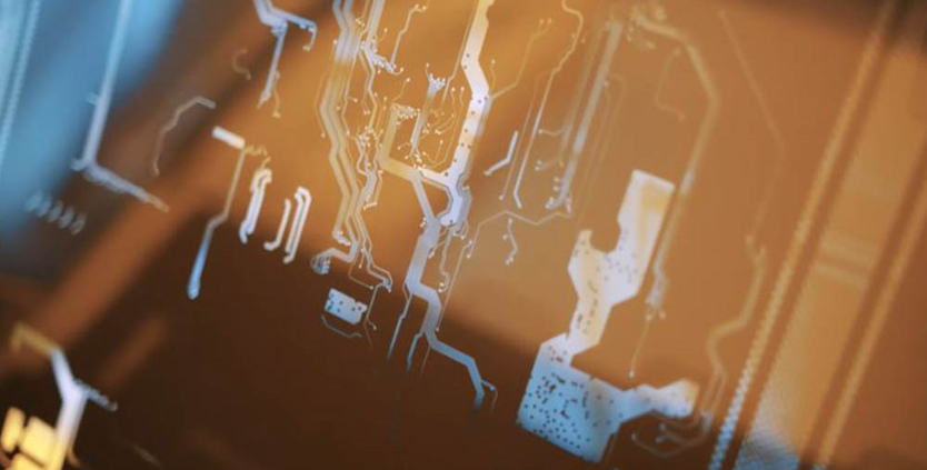
In the intricate world of electronics, the heartbeat of innovation lies within the Printed Circuit Board (PCB). These compact yet powerful components serve as the backbone of electronic devices, enabling the seamless flow of electrical signals. Ever wondered about the fascinating journey a PCB undergoes from inception to integration? Our upcoming article delves into the comprehensive process of PCB manufacturing, unveiling each step with precision and clarity. From the initial design phase to the intricate etching and assembly processes, we will guide you through the intricate web of techniques and technologies that transform raw materials into functional PCBs. Whether you’re a seasoned engineer, a curious enthusiast, or someone simply intrigued by the magic behind your electronic gadgets, join us on this journey through the fascinating world of PCB manufacturing. Get ready to witness the alchemy that turns copper, fiberglass, and solder into the sophisticated circuits that power the devices we rely on daily.
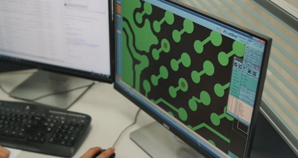
Everything starts with the Engineering Department. They receive the GERBER file, check it and compare it with the order, IPC standards, and supplier capabilities.
1 - Gerber File Check
ICAPE Group engineers carry out a Design For Manufacturability (DFM) review, check the data, the copper layers, the mechanical drawing, the specifications, and the line and space between the tracks. Once done, we create a file called ‘Technical Questions’ if necessary.
2 - DFM Review
This file is sent to the customer in order to propose a possible solution or improvement, such as different panelization techniques, solder mask type, design, base material, brand or specifications, and even different technologies in order to be feasible and cost-effective in the selected partner factories according to IPC standards.
3 - Partner DFM Review
Our partner factory enters the scene, receives the data, conducts a second DFM review, and starts combining Circuit designs on the production panel.
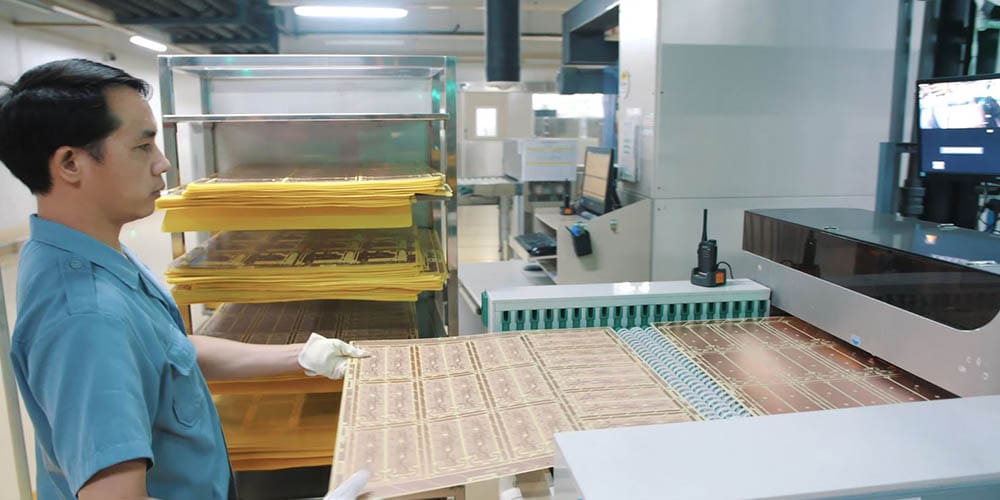
4 - Artwork Printing
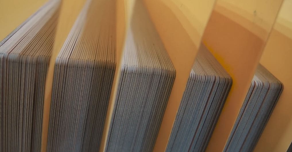
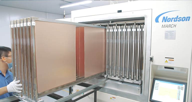
Each PCB layer is verified and transferred to the Printing artwork machine. We have one artwork for each layer: inner, outer, solder mask, legend printing, and also special layers like vias, peelable mask, carbon, etc. All those artworks can be used for thousands of panels.
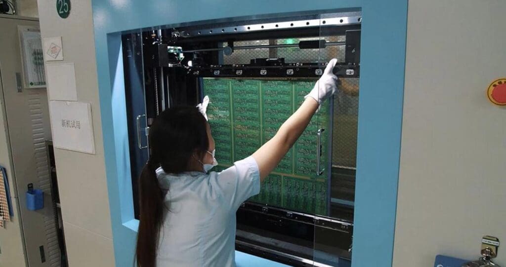
Discover how the panels are stored and prepared before going through the next stages of the manufacturing process!
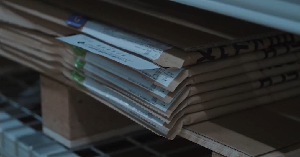
1 - STORAGE
Every PCB manufacturer does not produce basic raw materials such as prepreg or copper foil. All raw materials are supplied in accordance with ICAPE Group’s technical requirements. The materials are stored by types, total thickness, copper thickness, and brand.
2 - ORDER PREPARATION
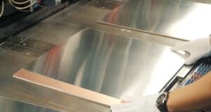
According to the order, the factory selects the required materials in the storage. The panels are unpacked and prepared to go through the process.
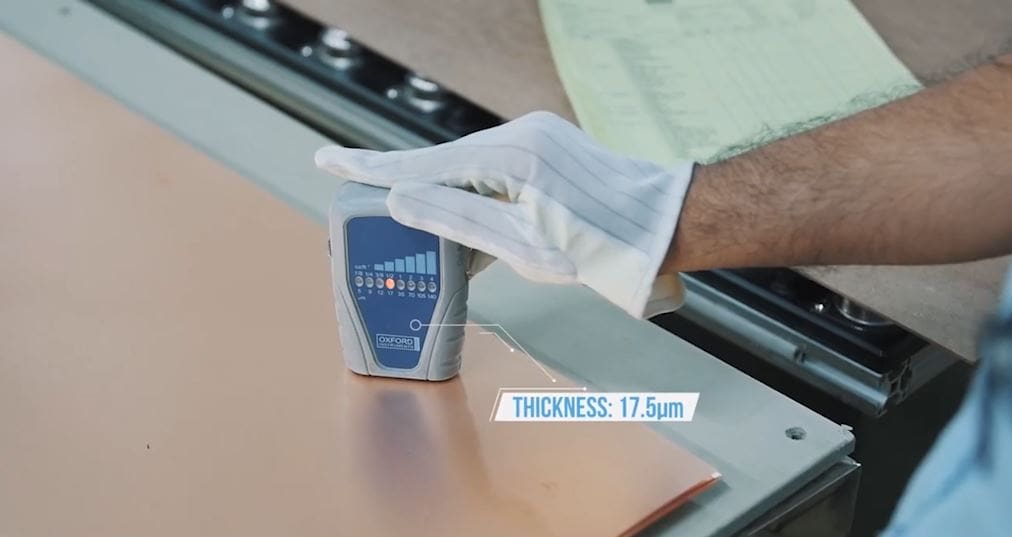
3 - CONTROLS
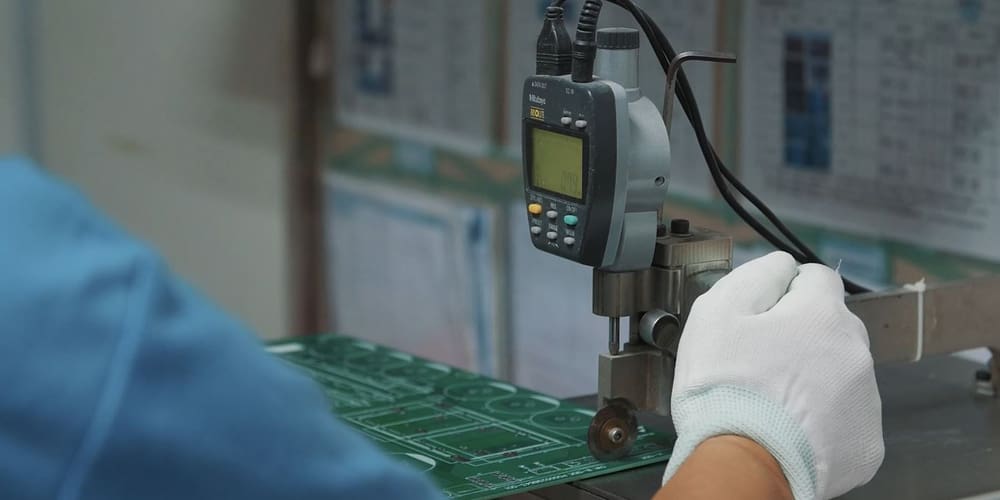
The inspection on each batch is an essential point. The copper and the total thicknesses are carefully checked with high precision tools, to make sure they respect the customers’ needs according to the technology in creation
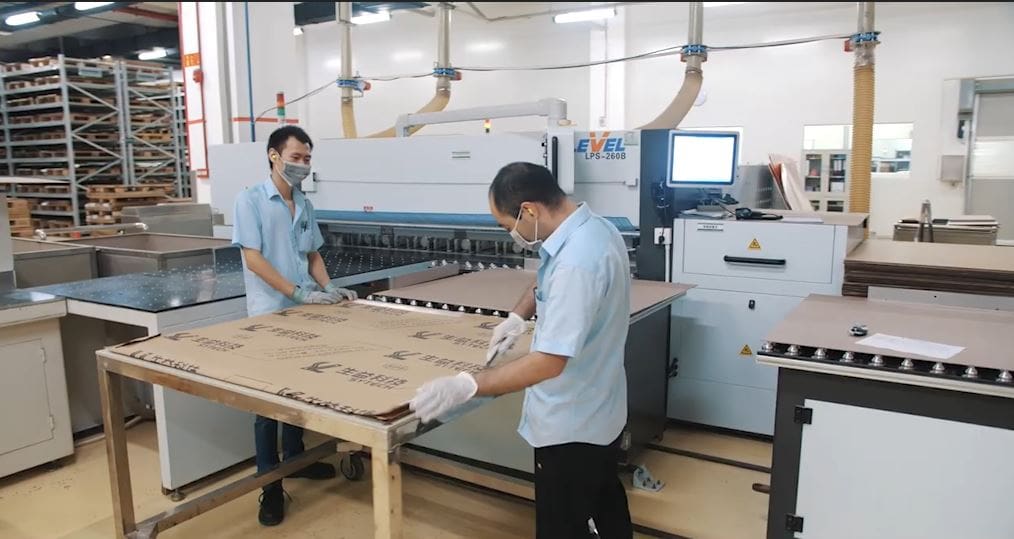
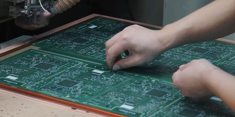
4 - CUTTING
The panel must be cut to production size. Nowadays, edge finishing and panel geometry are very important for CCD registration, and handling equipment.
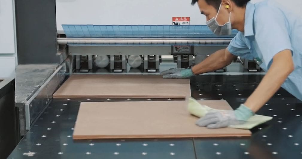
5 - CORNER FINISHING
Most companies have rounded the corners of the panels to reduce scratch issues and secure handling during the next stages of the manufacturing process
Jump aboard to discover the Lamination stage of the printed circuit board manufacturing process! After the inner Layer imaging stage, the boards go through registration and lamination. Follow us in our HDI factory in China!
1 - PREPARATION
The panels are washed to remove the corroded copper surface as well as potential fingerprints, dry film residues, carbonate and anti-foam residues from dry film stripping.
2 - MICRO ETCHING
Micro-Etching is a basic condition for obtaining a homogeneous and appropriate Brown or Black oxide treatment. The process will reduce the thickness of the copper from 0.2 to 1 micrometer.
3 - PBLACK OXIDE
Brown or Black Oxide treatment is used to provide better adhesion for the epoxy resin and to avoid any problem such as delamination.
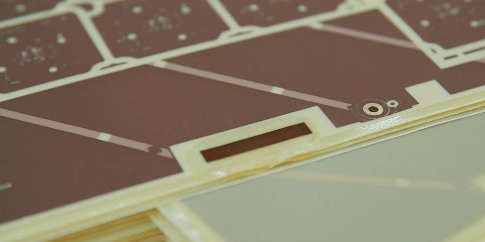
4 - INNER LAYER STACK UP
The operator stacks the inner-layer and prepreg on the gluing machine, allowing the stack-up to be glued together. Once glued, we move on to using the rivets. The riveting process is there to complete the registration and strengthen the inner layer and the prepreg together. This strengthens the stack-up and ensures that it won’t move during the lamination process.
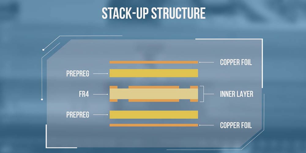
5 - STACK UP
The copper foil is sandwiched between a stainless-steel patch and a prepreg. This stainless-steel creates a hard and flat surface. The copper foil completes the stack-up. The panel is now composed at the top and the bottom by a copper foil and a prepreg surrounding the inner layer.
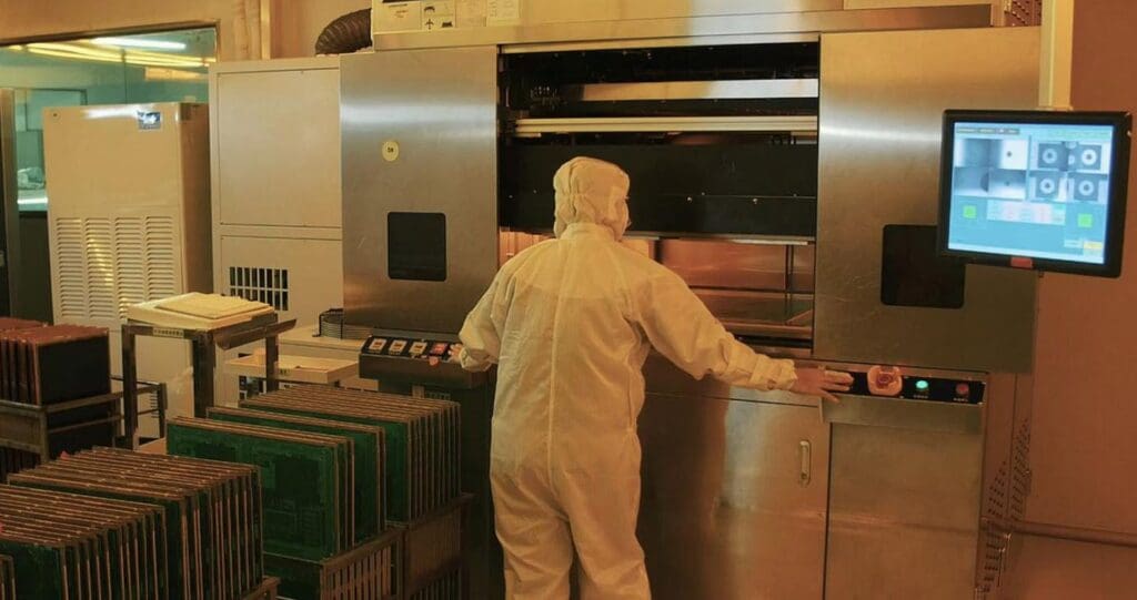
6 - LAMINATION
The stack-up is placed under extreme temperature depending on the data sheets of the materials. The pressure inside the lamination machine is 180 tons per square meter and the process will take up to 2 hours. After being exposed to high pressure and temperature, the layers form a single board, which is then moved to a cold press. Later, the panels will be unmolded.
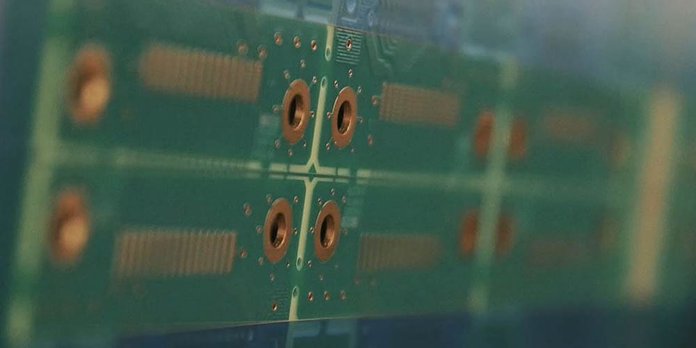
7 - HOLE REGISTRATION
These brand-new boards will be prepared with the registration holes using an X-Ray machine. They will then be deburred, chamfered and rounded at the corners.
Drilling
How challenging is the drilling process?
The fifth episode of our PCB Journey focuses on one of the most spectacular processes in our web series: drilling! It is not only the most impressive process but also the most irreversible! Indeed, this step must be very carefully implemented because even a small error can lead to a big loss. Discover the different stages of this process (mechanical or laser drilling, minimum diameter, or even controls) by following our two ICAPE Group experts in one of our partner factories in China.
1 - PREPARATION
For better accuracy and thermal management, specific materials are used such as Aluminum, Wood or Melamine at the top and the bottom of the stack up.
2 - TOOLS CONTROLS
The drill must be perfectly shaped and comply with the rules concerning the number of holes that can be performed by the same tooling. For high-tech PCBs, only new tools are used. For standard PCBs, the drills are sharpened up to 3 times before being renewed.
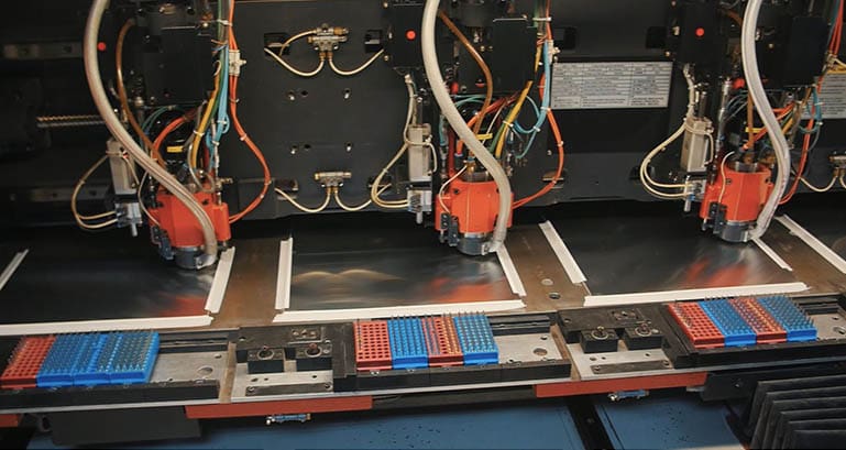
3 - MECHANICAL DRILLING
Depending on the series, the drilling machine manages one panel at a time for high-tech products. But it is also possible to install up to 4 panels at the same time, also depending on the thickness, with 1 to 6 drilling heads. During the 1990s, we used to drill a minimum diameter of 400 micrometers. Today, we can drill a minimum of 150 micrometers.
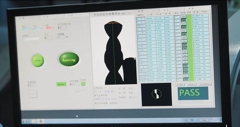
4 - CONTROLS
To help with visual control, on the edge of each board, all holes of different sizes are drilled and inspected after the drilling stage. The panels are also automatically checked with a hole verification machine. For the internal control, the boards go through the X-Ray machine, which checks the entire positioning in relation to the inner layer.
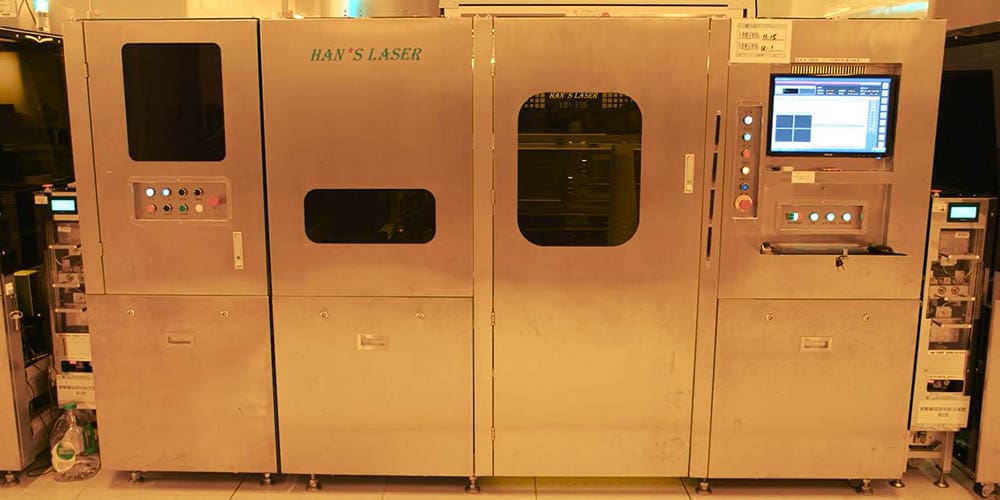
5 - LASER DRILLING
The laser drilling machine can generate vias holes between 50 and 150 micrometers. Current toolings are based on two main types of laser: UV or CO2 laser, and sometimes both depending on the process. Here, there is no top or bottom material, so we can only drill one panel at a time and the laser stops when it hits the copper on the N-1 layer. There are two main controls to ensure that the drill holes meet the requested dimensions and to check the cleanliness.
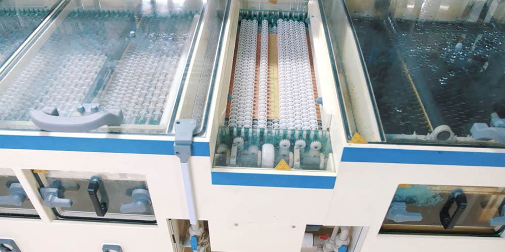
The chemical deposition of copper, also called electroless copper, creates the electrical connection between the inner layer and the outer layer.
1 - STANDARD CLEANING
Before depositing the chemical copper, the board must be clean. For the standard process, the first baths will clean up and remove all residue from drilling.
2 - PLASMA CLEANING
For high-tech products, the plasma process is preferable: capable of removing harder residues such as polyimides, High Tg-FR4, Teflon and RF Microwave materials. This optional process provides excellent roughness and wettability for chemical deposition of copper.
3 - PALLADIUM PLATING
Several chemical treatments exist to obtain conductive holes, we can use copper, palladium, graphite, polymer, according to the PCB technology in creation. The boards are immersed in a palladium bath also known as an activation bath to deposit a thin coat of palladium.
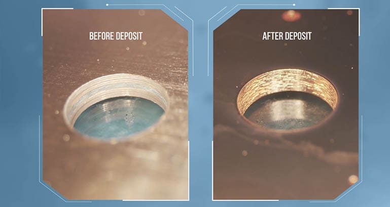
4 - COPPER PLATING
The panels are constantly moving through the bath to remove potential air bubbles that may have formed inside the holes. The palladium acts chemically so that a 1 to 3-micrometers deposit of chemical copper is attracted onto the entire surface of the panel and the recently drilled holes.
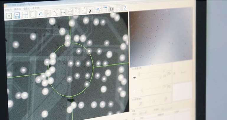
5 - CONTROLS
The control is carried out at the end of this process, mainly, a backlight test is performed to check the porosity and coating of the copper.
The Outer Layer Imaging is similar to the Inner Layer Imaging, but much more complex with the holes and the surface roughness. Let’s see how this spectacular step of the PCB manufacturing process is done!
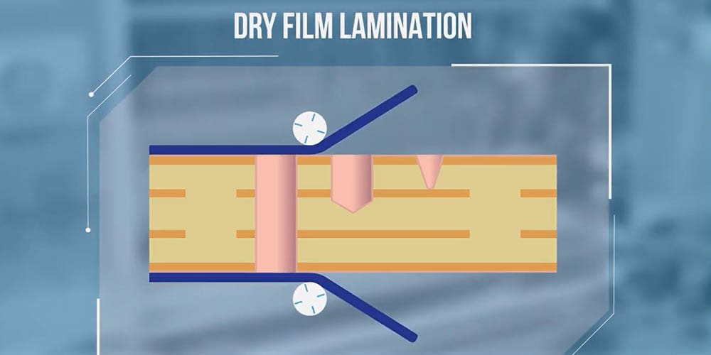
1 - PREPARATION AND LAMINATION
The surface is prepared: boards thinner than 500 micrometers undergo a chemical cleaning process, while thicker boards undergo a mechanical cleaning process using abrasive brushes. The boards are heated for better adhesion of the photoresist film. Then, the boards are coated with an automatic lamination on X and Y. The edge is cut directly by the machine.
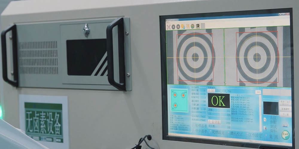
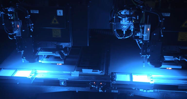
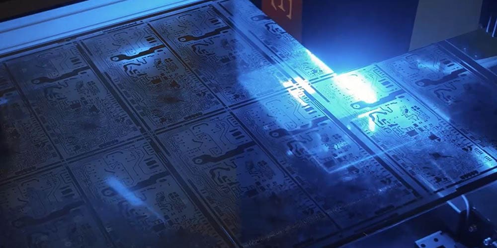
2 - REGISTRATION AND UV INSOLATION
For semi-automatic insolation, the artwork is checked again before being added to the machine. Registration is optically done between the holes and the targets with 2 or 4 CCD cameras. Once the panel meets the quality criteria, a vacuum is applied, then the board receives a blast of UV light between 1 and 20 seconds to polymerize the photoresist, creating an image of the circuit pattern.
3 - REGISTRATION AND LASER INSOLATION
For high-end products and high-density materials, Laser Direct Imaging is used. This machine is fully automatic, so loading, registration with 4 CCD cameras and transferring the layer image is done in seconds. LDI is also an important factor when close tolerances and tight registration are involved, such as 50 micrometers or less.
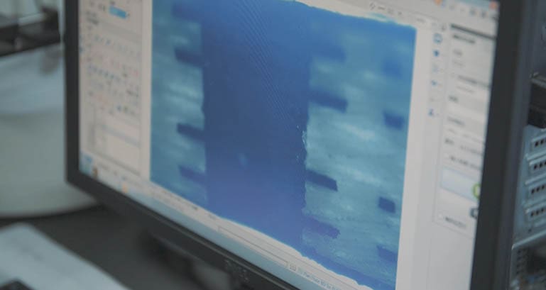
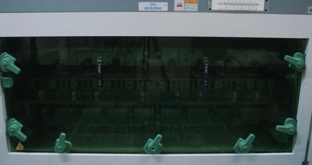
4 - DEVELOPING
Once the insolation is finished, the protection on the dry film is removed. The areas not exposed to UV Light or Laser are unhardened and will be dissolved in the developing sodium bath leading the boards to this beautiful blue color. The outer layer image is now printed, ready to receive electrolytic copper.
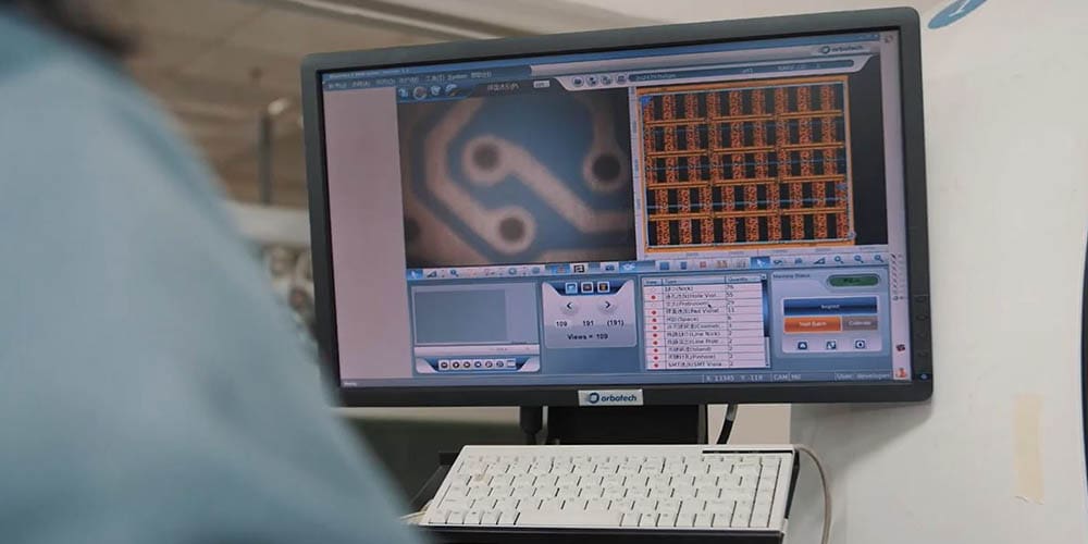
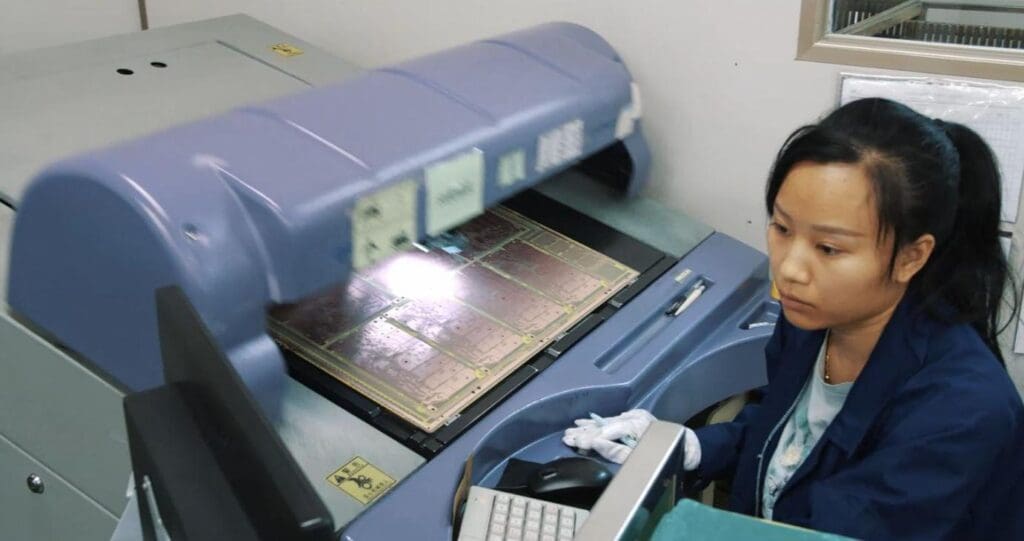
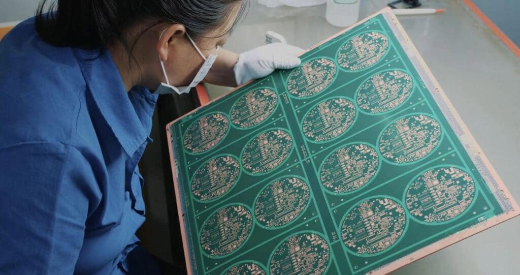
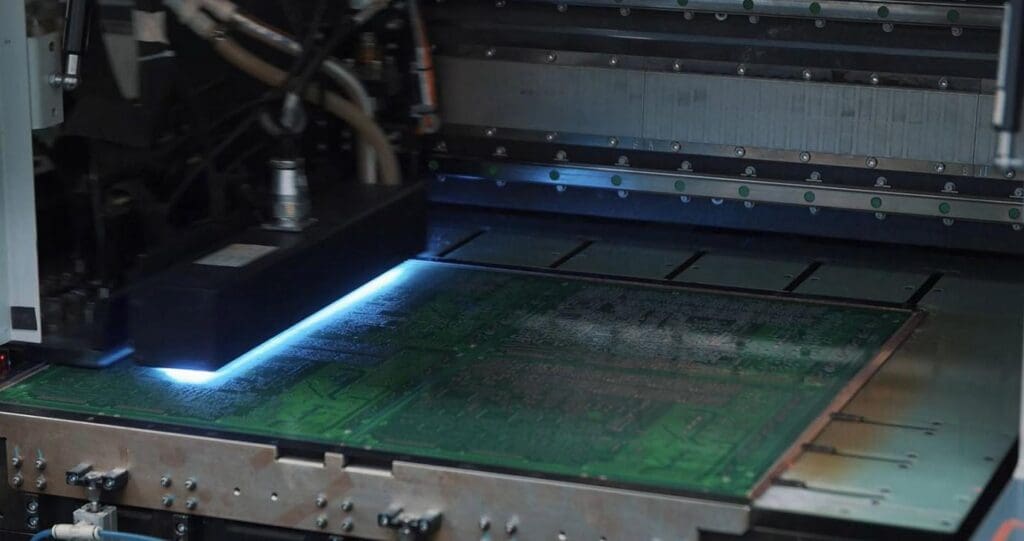
5 - AUTOMATIC OPTICAL INSPECTION
The Automatic Optical Inspection of the outer layers will confirm the total absence of defects, whether electrical opens or shorts. As with the Inner Layer, the original design from the GERBER file serves as a model for the optical camera. If the machine finds an inconsistency, a technician will assess the issue.
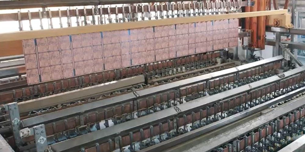
Copper can be deposited electrolytically on the board with two processes : Panel and Pattern process.
1 - PANEL PLATING
The copper is electrolytically deposited over the entire surface as well as inside the holes to improve flatness and distribution. Electrolytic copper creates electrolysis, which is a flow of electric current through a liquid that causes chemical changes. After several baths of 3 min each, electrolysis is created, the copper in the bath acts like an anode and the boards like a cathode.
2 - CONTROL
Copper is now thicker and more reliable with around 10 to 13 micrometers of copper. The next step for these boards will be the Outer Layer Imaging.
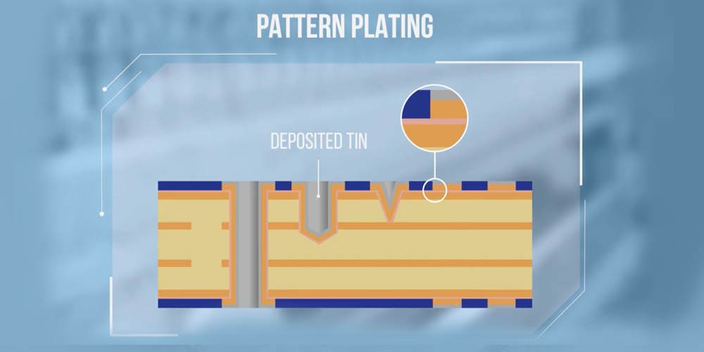
3 - PATTERN PLATING - COPPER DEPOSITION
The copper is deposited electrolytically, but in much greater quantities. To create a good connection and a good conductivity between the holes, the boards need at least 20 to 25 micrometers of copper inside the wall holes according to IPC standards. The copper, acting as an anode, is deposited on the boards during a 60-minute bath.
4 - PATTERN PLATING - TIN DEPOSITION
After a rinsing bath, the boards are immersed in the electrolytic tin which covers all the copper with a coat around 1 to 3 micrometers. The tin is essential to protect the copper during the etching process.
5 - CONTROL
Once they are completely covered, they are test with a non-destructive method to check the thickness of the coat.
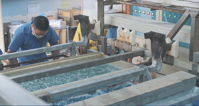
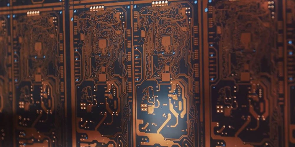
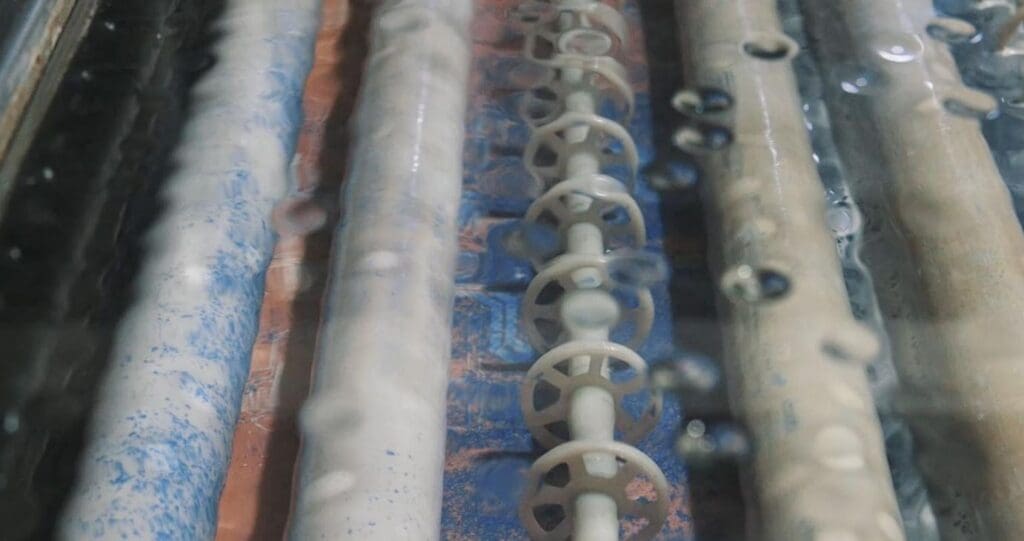
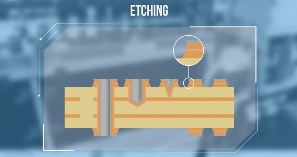
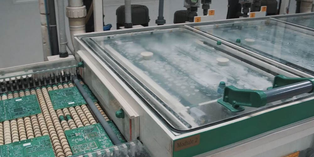
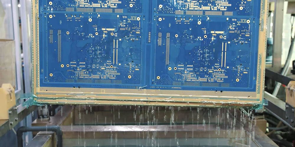
Etching is a complex chemical process that removes the unwanted copper and tin on the boards.
1 - FILM STRIPPING
The first step starts with the dry film. All the residue are dissolved, and the film is stripped away, leaving the unwanted copper exposed.
2 - ETCHING
The etching step starts in a bath of a chemical solution. The challenge is to avoid over-etching or under-etching which would prevent a straight wall from being obtained. As for the inner layer, the uncovered copper is etched away and defines the pattern. Here, the tin protects the copper and the holes.
3 - TIN STRIPPING
The tin is chemically removed and stripped away. Conductive areas and connections are now properly established.
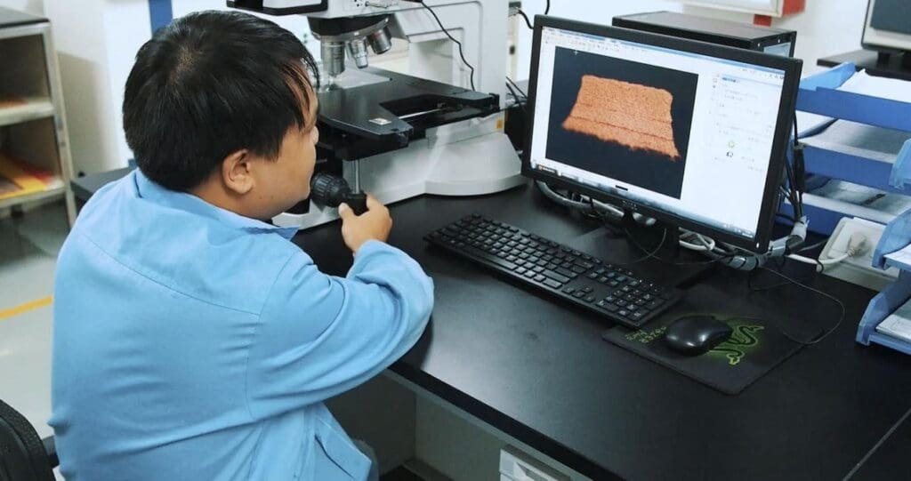
4 - CONTROL
A laboratory test is carried out to check the over-etching and the under-etching and to make sure that all unwanted copper layers have been removed with the exception of the resist layer.
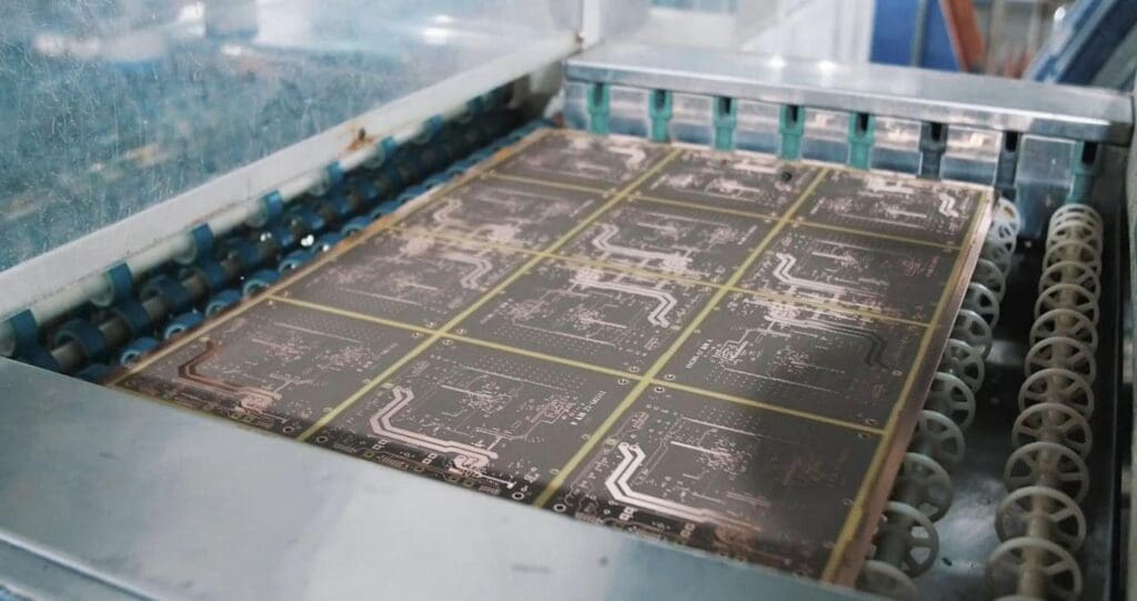
5 - AUTOMATIC OPTICAL INSPECTION
The Automatic Optical Inspection is carried out directly after etching and compared with the data to highlight any inconsistencies and guarantee the absence of defects. In some cases, a short circuit or electrical opening can be repaired at this point.
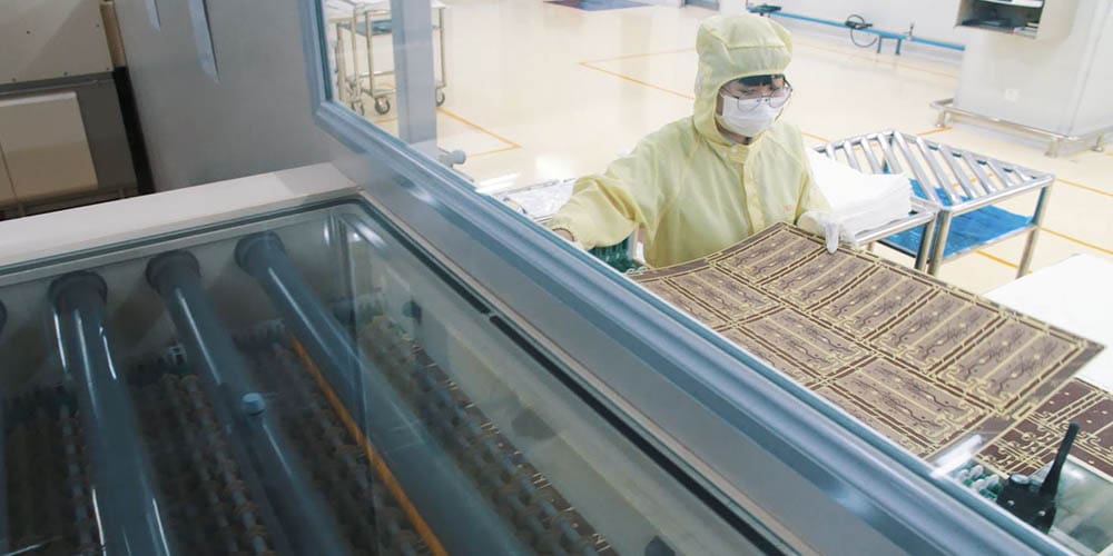
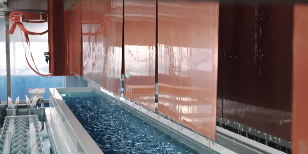
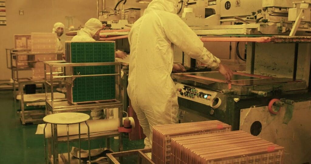
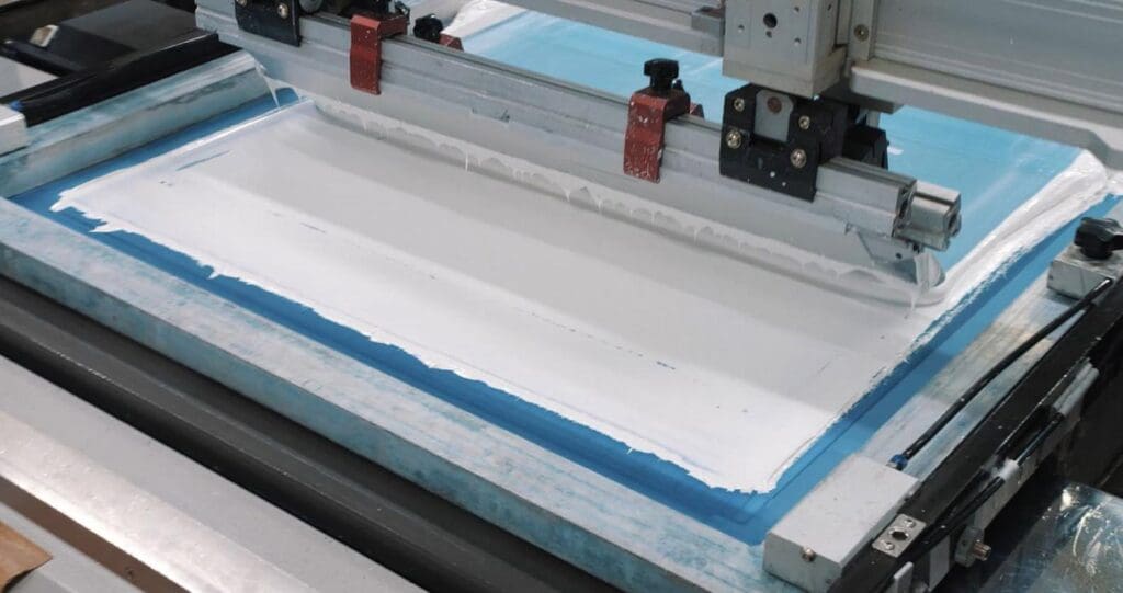
The solder mask has two interests. The first is to avoid the oxidation of copper and the second is to have perfect insulation between two traces of copper during the assembly process. There are different types of PCB soldermask, such as Epoxy Liquid, Liquid Photoimageable (LPI), or Dry Film. Let’s dive into it!
1 - COATING
There are different ways to apply the solder mask to a PCB: curtain, screen printing or electrospray deposition coating according to IPC standards. Before any solder mask application, the boards must be cleaned with a mechanical or chemical preparation in an over-pressurized cleanroom to prevent dust from entering from the outside.
2 - PRE-CURING
Once the panel is totally covered, it must be pre-cured. This step is essential and removes all the solvent from the ink. Without this step, registration will not be done properly.
3 -REGISTRATION/INSOLATION
For the soldermask, the insolation can be done with the registration with 8 CCD cameras and the artwork. The boards receive a blast of LED light for a few seconds to harden the soldermask where the artwork is clear. The insolation can also be done by LDI, Laser Direct Imaging. This time, no artwork is necessary because the machine directly insoles the selected locations with light beams and hardens the targeted location.
4 - DEVELOPING
The portions not protected and not hardened by the insolation are washed away. Here, in our example, the soldermask around the mechanical through-hole is removed.
5 - CONTROL AND CURING
After the developing phase, all the boards are controlled. Indeed, inspection is needed to check if there are any defective images, traces of ink on the pads or through the holes. Finally, the boards are exposed to a high temperature for one hour to cure the soldermask.
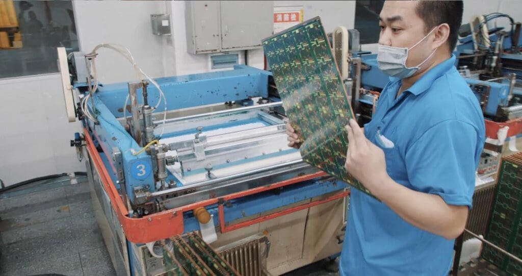
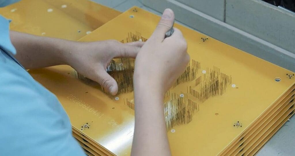
The legend printing process prints all of the vital information on the board, such as manufacturer marks, company ID numbers, and warning labels. Two methods are mainly used in this process: Screen printing, also known as silkscreen, and DLP for Direct Legend Printing with an inkjet printer. It looks easy, but like every step of the PCB manufacturing process, it requires precision.
1 - SCREEN PRINTING
As with most stages of PCB manufacturing, the artwork from the GERBER file is essential in the process of printing the legend pattern. The first method is screen printing also known as silkscreen process. Whether manual or automatic, they both require polyester screens stretched across aluminum frames. Both the aluminum frames and the panel are registered to guarantee proper alignment to avoid print ink on the copper pattern and to ensure that the soldering process will not be affected. The ink is pushed through the stencil onto the laminate.
2 - CONTROL
Once the PCB has been silk-screened with the correct information, visual inspection is carried out by the operator. In case of defect, the operator will assess the issue or remove the board from the production process
3 - CURING
If the result of the screen printing is good, the boards will be cured to harden the ink.
4 - INKJET
The second process of applying the legend text works like a conventional inkjet printer and is knows as DLP or Direct Legend Printing. Registration is done automatically by the machine. The inkjet printer sprays ink droplets on the panel to generate the image. These ink droplets are directly cured by UV lights.
5 - CONTROL
Visual control is also carried out by the operator to make sure the legend is correctly printed. Despite more modern equipment, DLP is preferable only for prototyping and small volumes while screen printing is much faster and used for mass production.
Surface finishing is a coating between a component and a bare board PCB. Mainly use for two reasons: Ensure the solderability during the populated phase and protect the copper from oxidation.
1 - OSP
OSP, stands for Organic Solderability Preservative. It is a water-based surface finish. Environmentally friendly, the boards are cleaned before going through the baths which will provide an excellent flat surface. This quick process does not require a lot of equipment which makes it a cost-effective surface finishing. OSP has a short shelf life and can be sensitive while handling. Consequently, the routing process is performed before the surface finishing application. To sum things up, OSP surface finish is environmentally friendly, provides a flat surface, is a cost effective solution that can be reactivated There are also drawbacks like short shelf life, can be sensitive while handling and this finish may expose copper during final assembly.
2 - LEAD-FREE HASL
Lead-free HASL is short for Hot Air Solder Leveling. it was one of the most popular finishes until a few years. Even if this finish is robust, the low price is also linked to its limitations. During this application, the entire panel goes through micro-etching to clean the board then receives a flux coating to help the surface finish adhere to it. Later, the board is immersed in liquid tin solder and is removed by using two air knives which blow hot compressed air across the surface of the boards. The lead-free solution is an indisputable advantage for the high-reliability products. But with more and more HDI boards, this process provides uneven surfaces and is not suitable for fine pitch components. To sum things up, Lead-Free HASL surface finish is a widely available technology, a low cost solution with good durability. There are also drawbacks such as the surface which may be uneven, it is not suitable for fine pitch components and the process can be a thermal stress for the boards.
3 - ENIG
ENIG goes for Electroless Nickel Immersion Gold. This process requires tape to cover the contours of the circuit in order to avoid excessive gold deposition and because ENIG is an expensive finishing process. The panel is immersed in several baths, first a layer of 3-6 micrometers of nickel is electrodeposited to increase adhesion. Then, a minimum of 0.05 micrometer of Gold is electrodeposited as well on the panel. An immersion finishing provides excellent flatness and the use of gold provides a strong solderability. To sum things up, ENIG surface is ideal for bonding, has a strong solderability, provides a flat surface and has a good shelf life. There are also drawbacks, mainly the fact that this surface is a complex process not a cost-effective solution.
4 - HARD GOLD PLATING
For the Hard Gold Plating, the entire panel is covered by tape. Only the part that requires the application of a surface finish is removed. Unlike ENIG, in this case, the copper thickness can vary by controlling the duration of the plating cycle. The nickel is first electrodeposited, then the gold is deposited according to the customer’s request. The gold thickness provides an excellent shelf life but also one of the most expensive surfaces finishing options. To sum things up, Hard Gold Plating surface finish has mechanical properties, excellent shelf life and provides a flat surface. There are also drawbacks such as high cost, poor solderability and the process is complex.
5 - IMMERSION TIN
Immersion Tin is a metallic finish deposit. The boards are immersed in several chemical baths to create the best adhesion for the tin. The immersion will provide perfect flatness and the tin will best protect the underlying copper. It is a cost-effective option, but the strong affinity between the tin and the copper can lead to tin whiskering. Immersion Tin surface finish is widely available, provides a flat surface, it is a cost-effective solution, has good shelf life and is reworkable. There are also drawbacks such as the rework which is limited, handling can be sensitive and there are possibilites of tin whiskering. ICAPE Group calls specifically for a high-tech finishing product a partnership with German-based factories to realize the Immersion Tin who suits which corresponds to the expectations of the German automotive industry.
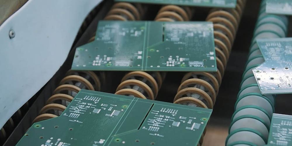
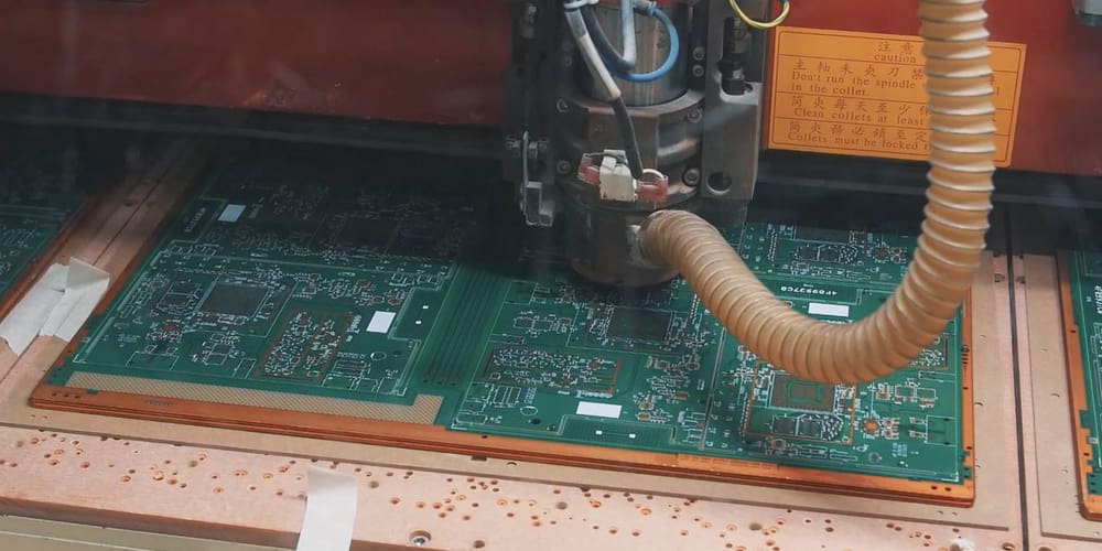
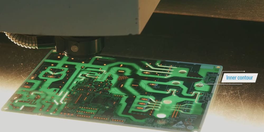
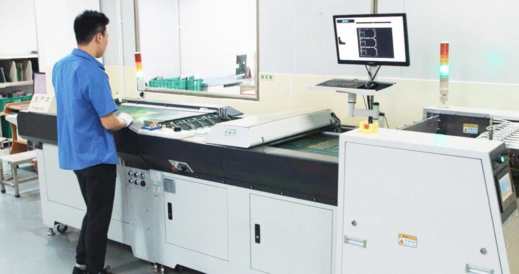
The purpose of the routing process, also known as profiling, is to cut each circuit board out of the production panel. Indeed, even if all the circuit boards are on the same panel, they do not necessarily all belong to the same customer
1 - PREPARATION
The operator stacks up to 4 panels, in the same ways for the drilling process. In this case, the routing process requires a milling machine and bits with a different number of heads: 1, 2, 4 or 6 heads.
2 - ROUTING
Inner and outer contours of the PCB are created during this process. At the same time, the boards are cleaned to ensure that no dust remains as a result of this operation. At the end of the cycle, the operator removes all the parts from the table and the circuit boards are now depaneled. Depending on the customer’s request, the boards can also be milled without being depaneled
3 - CONTROL
The operator monitors the dimensions of the milling process with an optical camera to ensure that the inner and outer contours have been milled properly and have not affected the circuit.
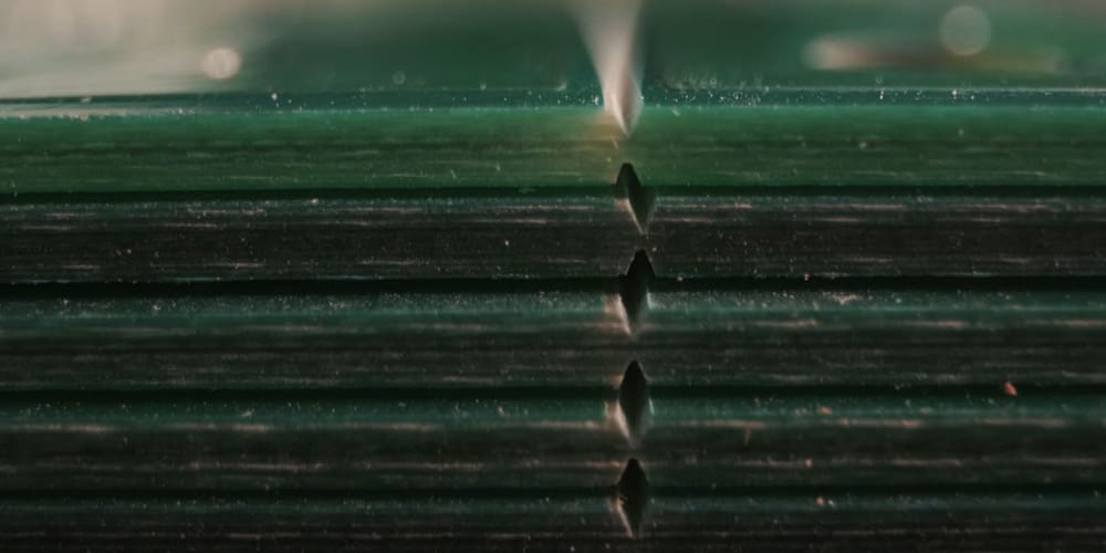
4 - V-CUT
After routing, V-Scoring or V-cut is used to pre-cut the PCB on the customer panel so that the boards can be separated after the populating stage. This is the main objective of this step. The boards are then easy to snap.
5 - CONTROL
Once completed, controls are carried out with a V-cut tester to measure the V-cut depth according to the GERBER file.
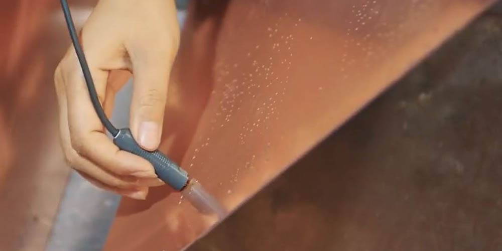
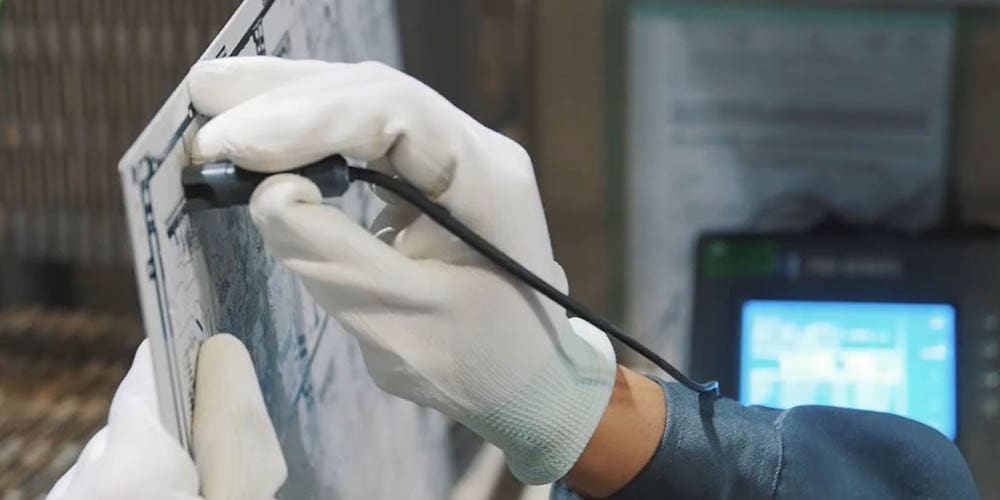
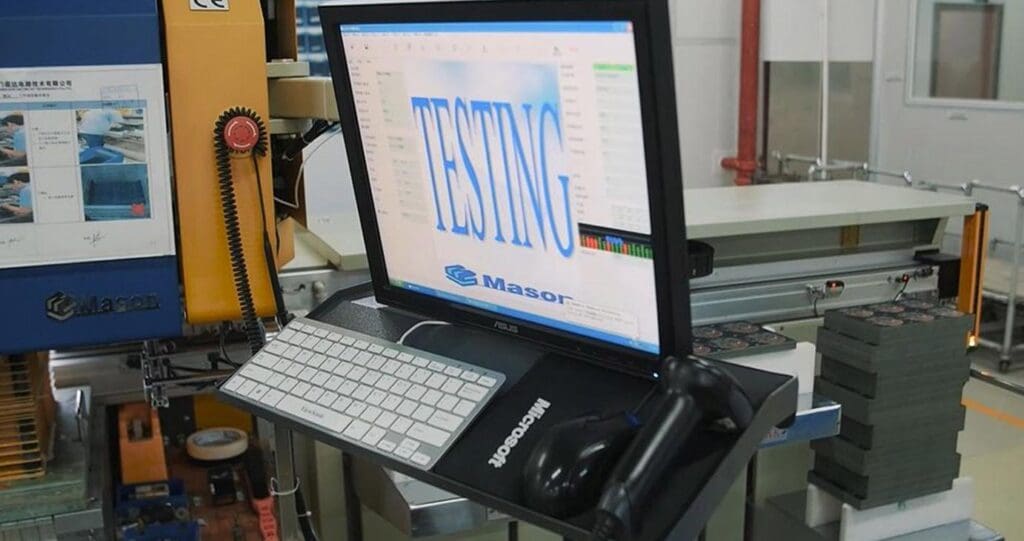
These tests are carried out to ensure there are no shorts and opens on the circuit boards. There is two types of machines with differents advantages: the “flying probe” and the “bed of nails”.
1 - FLYING PROBE
The GERBER file is read by the machine, the operator place the boards in panel or alone. Then the 4, 6 or 8 heads, distributed on each side, start their job: send electrical charge to the circuitry while, each contact pads will be touch continously to make sure there is no open or short circuit. In this case, an operator will intervene to solve the problem.
2 - PROS AND CONS
The tooling is cost effective, it is most common to use it for prototyping & small series. It is also suitable for HDI PCB but the principal contraints is to change each time the circuit boards manually, which extends a lot cycle operation.
3 - BED OF NAILS
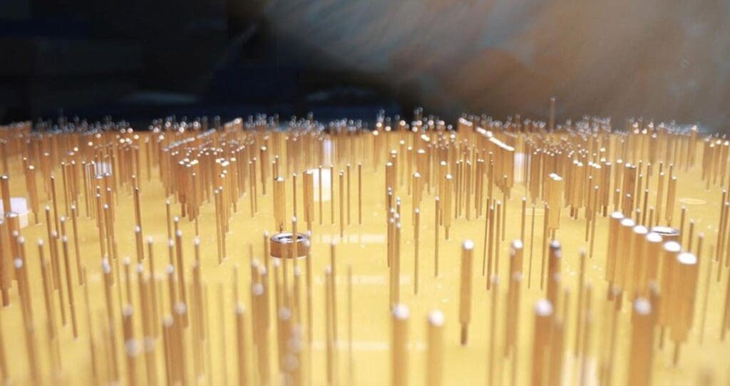
The universal grid test also know as Bed-of-Nails required a test fixture. The tests fixture is designed base on the GERBER file, so it’s different for each PCB. The operator must put numerous pins of various size to cover all the testing area. The preparation is extremely expensive and tedious! The holes are aligned to the test points of the PCB and all the test points are checked at the same time, which makes this very fast and reliable.
4 - PROS AND CONS
As for the Flying Probe, the Bed-Of-Nails got its pros and cons, This electrical test is perfect for the mass production for its processing speed between each PCB. Nevertheless, the expensive tooling, the tedious preparation and the density limits should be taken into account.
5 - TESTS COMPLETED
So now that the electrical test is complete, we are sure that the circuitry is corrrect. Coming up next is the final inspection.
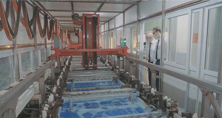
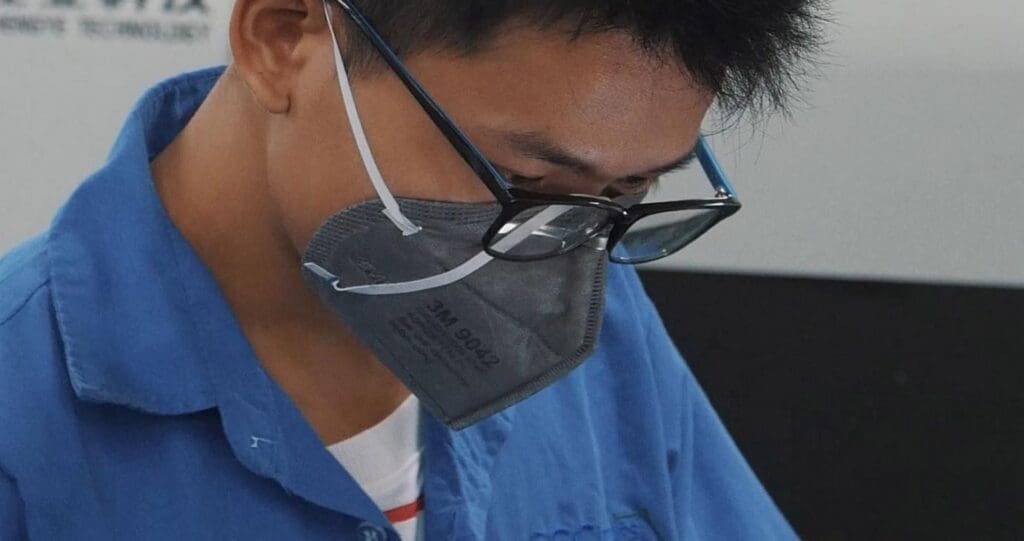
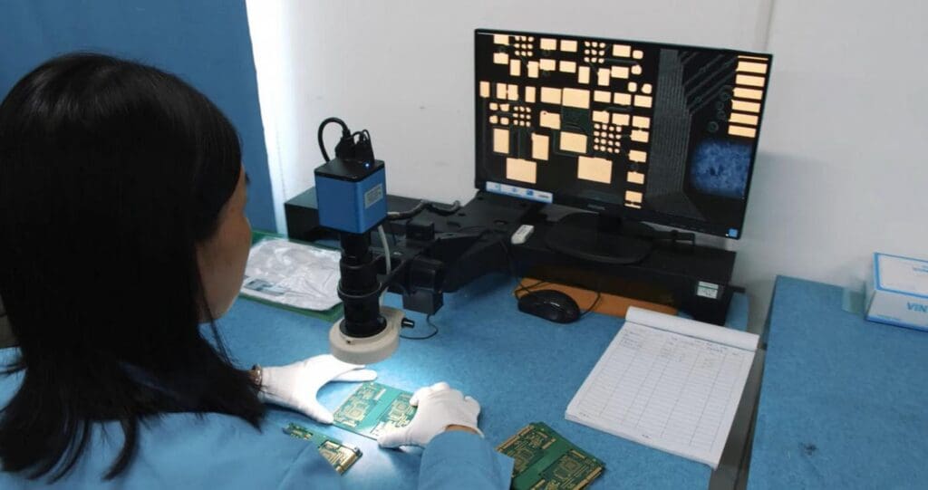
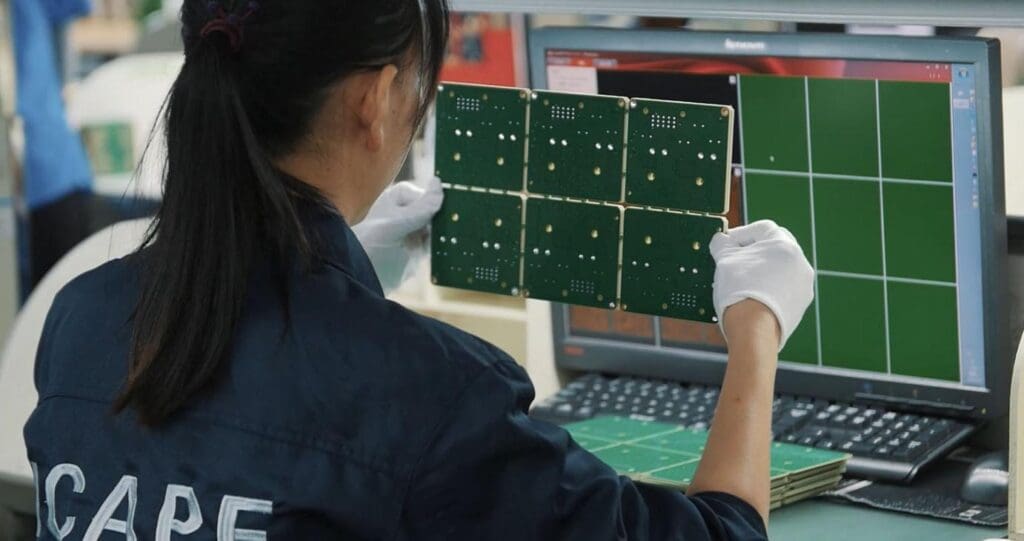
This is a crucial step in the manufacturing process. The supplier will control the entire board here, from the functional aspect to the cosmetic aspect. And they check everything compared to ICAPE’s requirements and of course even to the IPC standards. Besides, we also have an ICAPE controller on site who will check everything during the process, as well as before packing and shipping.
1 - AUTOMATIC INSPECTION
Each board goes through the Automatic Visual Inspection machine (AVI). This machine checks the PCB faster than human eyes, and detects inconsistencies compared to the GERBER file. Then, the board are placed on the Automatic Hole Checker to detect if some holes have irregular sizes.
2 - SUPPLIER INSPECTION
All the boards are visually checked by keen-eyed inspectors to control every specification. The evaluations carried out by our partner factories are monitored by ICAPE Group in-house inspectors who are constantly present in these factories.
3 - PQC AND QA TEAMS
Our Quality Control teams (QC) and our Quality Assurance teams (QA) go to our factory partners to perform the final controls themselves. Quality Assurance is process-oriented, and prevents defects by securing the processes used to manage and create deliverable PCBs. Quality Control is product-oriented and determines the end result is what was expected.
4 - ICAPE LABORATORY
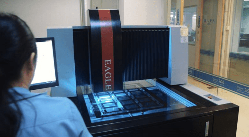
Our laboratory is able to perform many tests such as micro section analysis, controlling the copper deposit on the surface of the hole, checking the ionic contamination residues, controlling the surface plating, the roughness, controlling the impedance of the PCB and the signal integrity. Aging test and thermal shock can also be performed on the PCB to verify is reliability to harsh conditions.
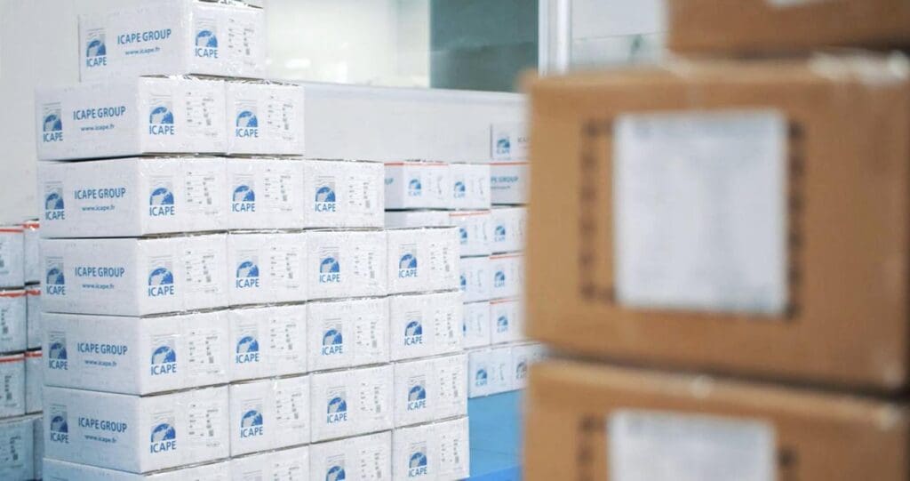
5 - PACKAGING
Once the inspection is complete, the boards are washed in de-ionized water to remove any dust and contaminants that may have remained on the PCB. Then, the boards are carefully packed in vacuum packaging. Label shipping is added and they are ready for shipping. The boards can be shipped according to the mode of transport requested, it can be DDP, DAP whether by Air, by trains or by boats.
Welcome
To ensure compliance with European data protection regulations, please verify you are in Europe.