
PCB MANUFACTURING
The comprehensive guide
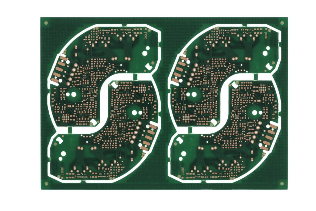
What is PCB?
What Does PCB Mean?
A Printed Circuit Board (PCB) is a fundamental component in electronic devices, providing a platform for connecting various electronic components. PCBs are essential for establishing electrical connections and mechanical support within electronic devices.
How Do PCBs Work?
To understand how PCBs work, think of them as the central nervous system of an electronic device. The copper traces act as conductive pathways that carry electrical signals from one component to another. The electronic components, like microchips, resistors, and capacitors, are soldered onto the PCB, allowing them to be interconnected.
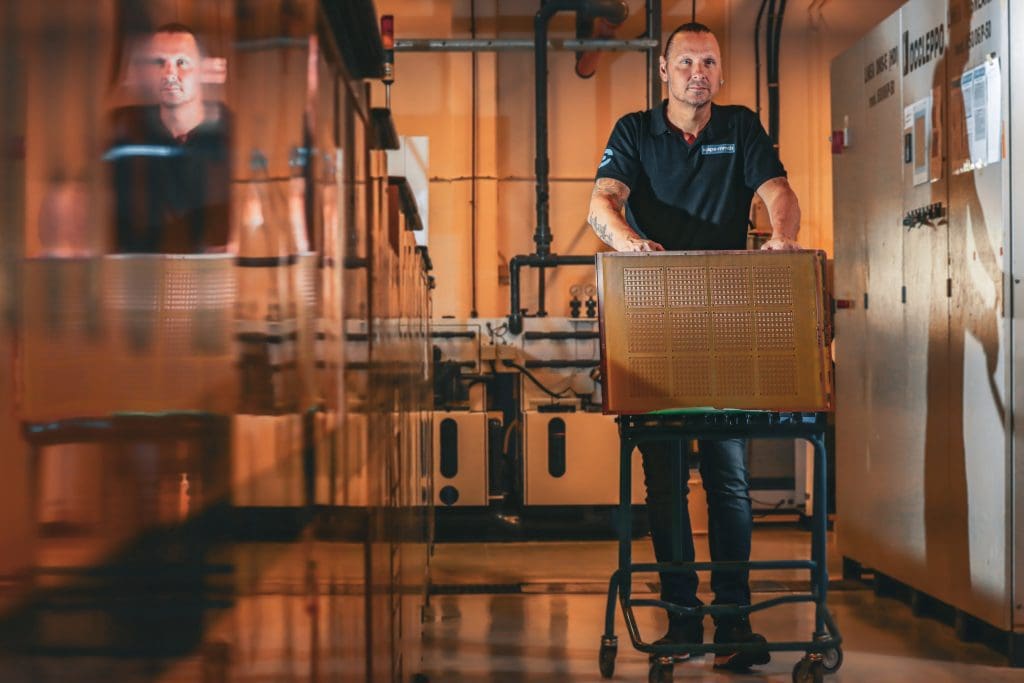
How are circuit boards made?
This organized approach to connecting components ensures that signals travel the intended path, avoiding interference and electrical noise. In essence, PCBs enable devices to function as intended.
PCB Fabrication Process
Discover the process, from the initial concept to the final product. Let’s dive into the world of printed circuit boards and explore the fascinating steps that bring your electronic devices to life!
Steps in PCB Manufacturing
The PCB manufacturing process involves several crucial steps:
Design Phase
- Schematic Design: Engineers create a schematic diagram of the circuit.
- PCB Layout: The schematic is transformed into a physical layout.
Printing the Circuit on the Board
- Image Transfer: The PCB layout is transferred onto the board.
- Etching: Excess copper is removed, leaving the circuit traces.
Adding Layers
- Multilayer PCBs: Multiple layers are laminated together.
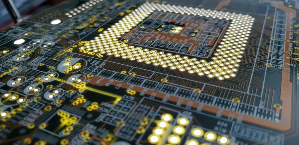
- Drilling: Holes are created for component leads and vias.
Plating and Copper Deposition
- Electroplating: A layer of copper is deposited on the PCB’s surface.
- Tin Plating: A protective layer of tin is applied to the copper.
Component Placement
- Surface Mount Technology (SMT): Components are placed on the board using machines.
- Through-Hole Technology (THT): Components with wire leads are inserted into holes.
Soldering
- Soldering: Components are attached to the board using solder.
- Reflow Soldering: Components are soldered using a reflow oven.
Testing and Quality Control
- Electrical Testing: PCBs are checked for connectivity and functionality.
- Inspection: Visual and automated checks ensure quality.
Final Assembly
- Additional components like connectors and enclosures are added.
- Comprehensive testing guarantees the device functions as intended.
PCB Manufacturing Costs
How Much Does the PCB Manufacturing Process Cost?
The cost of PCB manufacturing depends on various factors:
Design Complexity
More complex circuits may require additional manufacturing steps and layers, increasing costs.
Material Choices
The selection of materials, such as FR-4 or high-frequency laminates, impacts costs.
Quantity
Ordering in bulk often reduces the cost per PCB due to economies of scale.
Turnaround Time
Faster production may come at a higher cost.
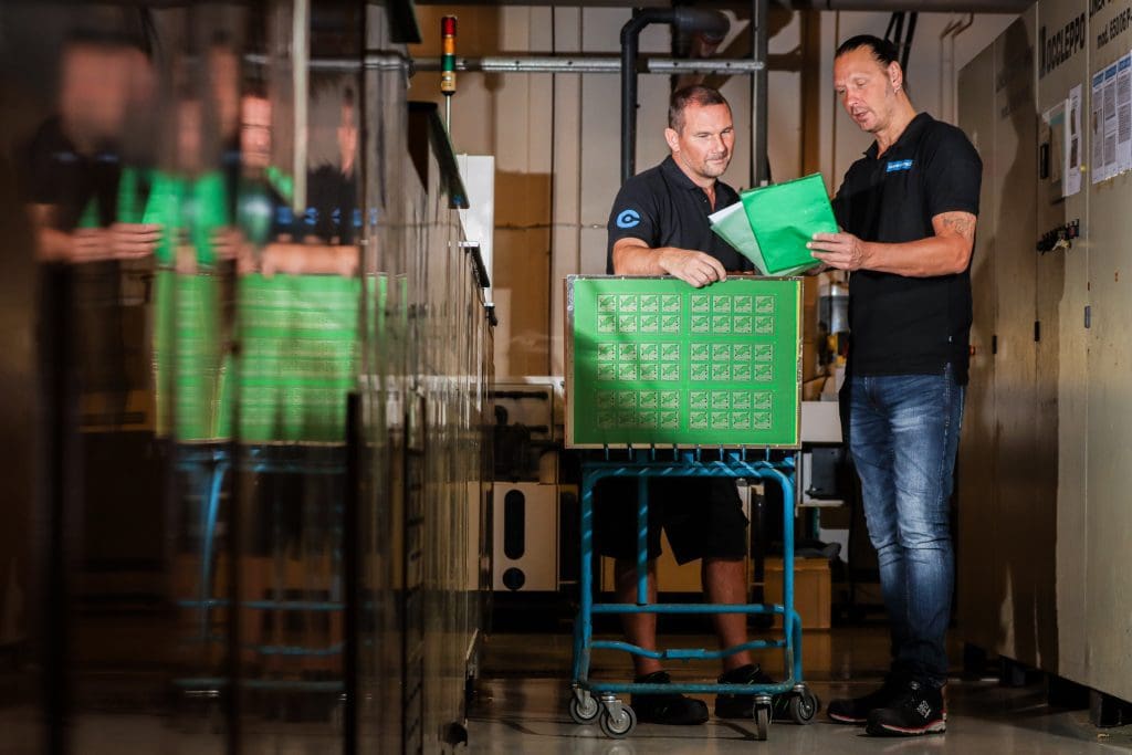
How is a pcb manufactured step by step?
ICAPE Group has produced a video series to explain each step of the manufacturing process.
How Are PCBs Made?
Material Selection
PCBs are typically made from materials such as FR-4, fiberglass epoxy laminate, which are clad with copper foil. The choice of material depends on the PCB’s intended application and electrical characteristics.
Design and Layout
Engineers create the PCB layout using specialized software and export Gerber and drill files for the manufacturer. A Gerber file is a standard file format used in the printed circuit board (PCB) manufacturing industry. It is named after the Gerber Scientific Instrument Company, which originally developed the format. These files are used to communicate the design specifications to PCB fabrication facilities, allowing them to produce the physical circuit boards accurately.
Gerber files are essentially a set of 2D vector images that describe the different layers of the PCB design. Each layer, such as the top copper layer, the bottom copper layer, solder mask, and silkscreen, is represented as a separate Gerber file. These files contain coordinates, shapes, and attributes that define the layout and features of the PCB.
Typically, PCB design software generates Gerber files as part of the design export process. These files can be sent to a PCB manufacturer for fabrication. The manufacturer uses the Gerber files to create the photomasks and other tools needed to produce the PCB according to the designer’s specifications.
The layout includes the arrangement of components, traces, and any required inner layers. Design rules must be respected to avoid any problems during the manufacturing process or any reliability issues in the final product.
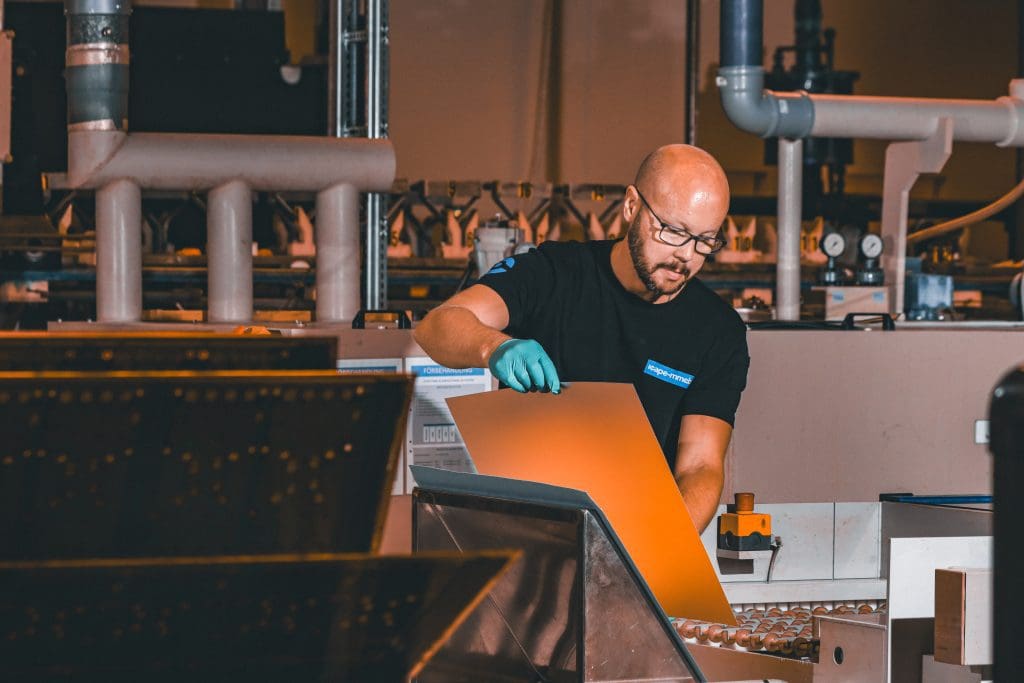
Printing the Circuit
The Gerber files are used to create photomasks, which are essentially templates used in the exposure step. Each photomask corresponds to a specific layer of the PCB design, such as the copper traces, solder mask, and silkscreen.
The PCB layout is printed onto a copper-clad board, forming the circuit’s pattern. A layer of photosensitive material, called photoresist, is applied to the bare copper-clad board. The board is then pre-baked to ensure the photoresist adheres properly.
Then, the board is immersed in a chemical developer solution that washes away the unexposed (unhardened) photoresist, leaving behind the desired patterns of hardened photoresist.
Etching
Chemical processes remove excess copper, leaving behind the circuit traces. The board is placed in an etching solution that removes the exposed (unprotected) copper. The hardened photoresist acts as a mask, protecting the copper traces and features that were defined during exposure. This process leaves only the desired copper traces and component pads on the board. The remaining photoresist is stripped away, leaving the clean copper traces exposed.
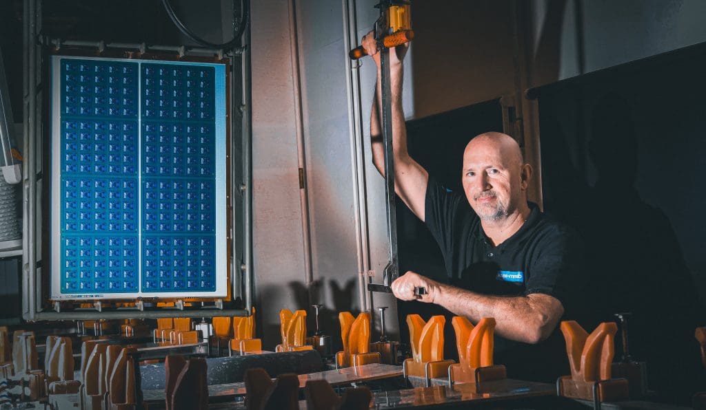
Adding Layers
The process of adding layers involves laminating multiple thin sheets of copper and insulating substrate together, creating a composite structure. This allows designers to achieve increased routing density and accommodate a higher number of components, making it an essential step in the evolution of modern PCBs.
Registration Challenges: However, with the benefits of additional layers come registration challenges. Achieving precise registration, or alignment, of each layer during the manufacturing process is critical to ensure that conductive pathways and components align accurately across layers. Misalignment can lead to short circuits, impedance variations, and compromised signal integrity.
Mitigating Registration Challenges: Advanced manufacturing technologies, such as automated optical alignment systems, play a crucial role in mitigating registration challenges. These systems use high-resolution cameras to precisely align and register each layer, minimizing the risk of misalignment. Additionally, manufacturers employ stringent quality control measures, including automated inspection processes, to detect and rectify registration issues before the final product is assembled.
Technological Advancements: Innovations in manufacturing equipment and techniques continue to address registration challenges. Laser drilling and imaging technologies, for instance, contribute to finer feature sizes and improved layer-to-layer registration accuracy, enabling the production of high-density, reliable PCBs.
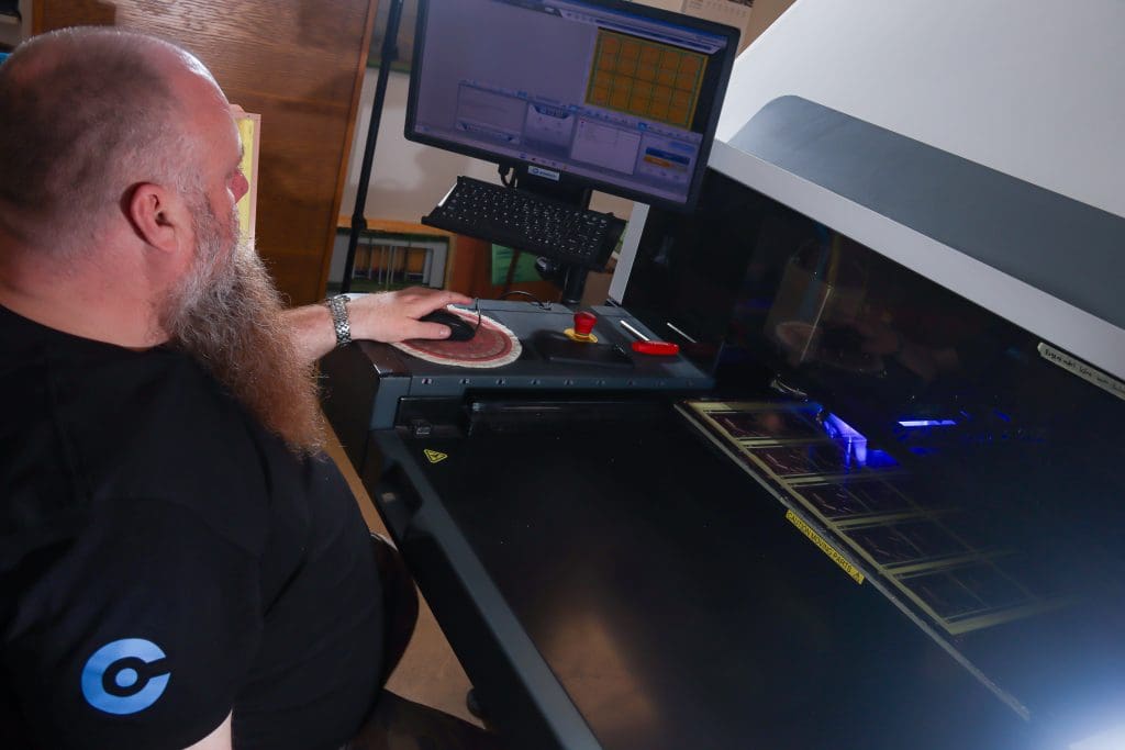
Final inspections
Testing and quality control play pivotal roles in the printed circuit board (PCB) manufacturing process, ensuring the electrical connectivity and the reliability and functionality of the PCB. Here’s an overview of the key aspects of testing and quality control in PCB manufacturing:
Visual Inspection: Visual inspection is the initial step, where trained professionals examine the PCB for any visible defects. Automated optical inspection (AOI) systems are often employed for precise and efficient visual assessments.
Electrical Testing: Electrical testing verifies the functionality of the PCB by checking for continuity and proper electrical connections. Two common methods are in-circuit testing (ICT), which assesses individual components and connections, and functional testing, which evaluates the overall functionality of the assembled PCB.
Flying Probe Testing: Flying probe testing involves the use of automated equipment with moving probes to test PCBs without the need for dedicated test fixtures. This method is especially useful for prototypes and low-volume production, allowing for quick and flexible testing..
X-Ray Inspection: X-ray inspection is employed to examine the internal structure of a PCB, identifying potential defects such as hidden circuit issues, voids, or misalignments. This non-destructive testing method is particularly valuable for inspecting complex and densely populated PCBs.
Thermal Stress Testing: Thermal stress testing evaluates the PCB’s performance under varying temperature conditions. This ensures that the PCB can withstand temperature fluctuations without compromising its structural integrity or electrical functionality.
Quality Control Documentation: Robust quality control documentation is essential for traceability and accountability. This includes maintaining records of inspection results, testing outcomes, and any corrective actions taken during the manufacturing process.
By implementing rigorous testing and quality control measures, PCB manufacturers can identify and rectify issues early in the production process, ensuring that the final products meet industry standards and customer expectations for reliability and performance.
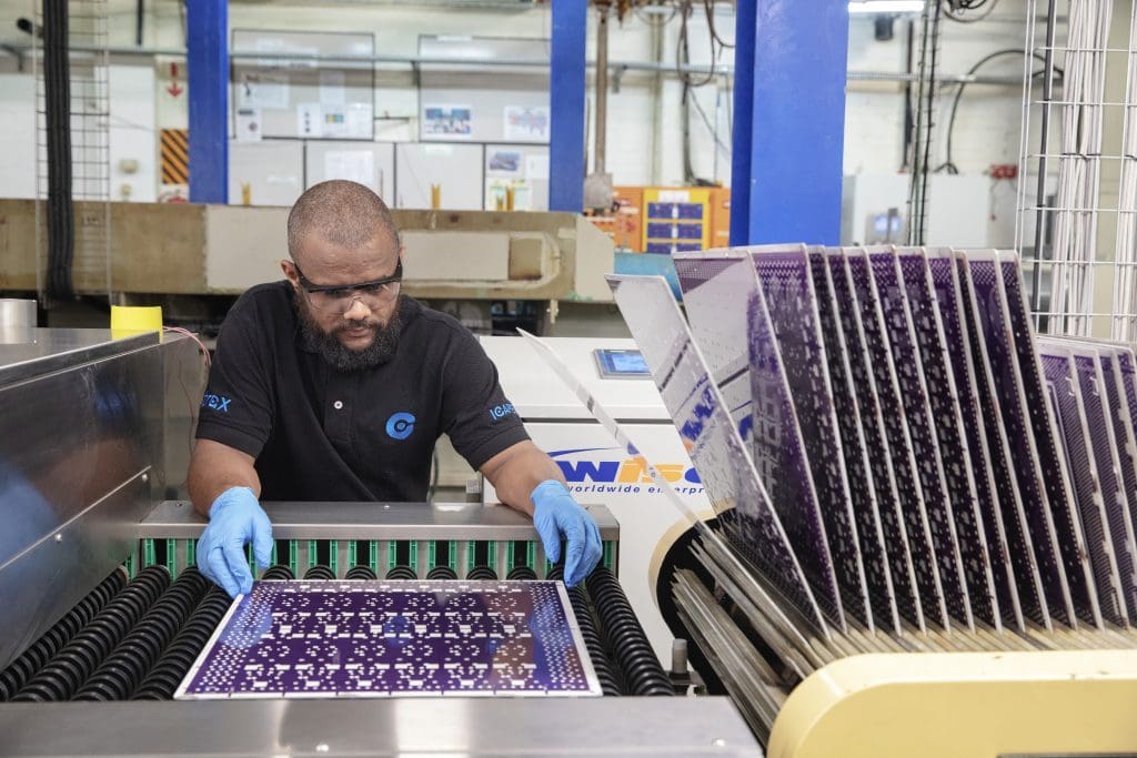
Which machines are used to manufacture Printed Circuit Boards ?
Manufacturing printed circuit boards (PCBs) involves a variety of machines and equipment designed to carry out different stages of the PCB production process. Here are some of the key machines and equipment commonly used in PCB manufacturing:
Printers and Plotters: These machines are used to transfer an image, by way of a phototool or direct imaging, to the photoresist material that has been applied to the pcb production panel. They print or plot the circuit pattern, including the positions of components and the routing of copper traces.
Etching Equipment: Etching machines remove excess copper from the substrate, leaving behind the desired circuit traces. This process is typically done using chemical etchants, with the etching equipment controlling the process.
Lamination Machines: For multi-layer PCBs, lamination machines are used to align and bond multiple layers of copper-clad substrates together. They ensure a secure and stable bond between the layers.
Drilling Machines: Drilling machines are used to create holes in the PCB. These holes are essential for connecting different layers of the board or for mounting through-hole components.
Plating Equipment: Plating equipment adds a layer of copper to the walls of the holes¨and circuit pattern. This is known as the electroplating process and is crucial for creating reliable electrical connections.
Soldering Machines: Surface mount technology (SMT) and through-hole technology (THT) components are soldered onto the PCB using soldering machines. Examples of the machines are reflow ovens for SMT and wave soldering machines for THT.
Testing and Inspection Equipment: Various testing and inspection machines, including automated optical inspection (AOI) and in-circuit testing (ICT) machines, are employed to ensure the quality and functionality of the PCBs. They help identify defects and verify electrical connections.
Pick-and-Place Machines: Pick-and-place machines are used to precisely position surface-mounted components onto the PCB. They play a crucial role in high-speed and high-precision assembly processes.
3D Printers: Some manufacturers use 3D printers to create custom PCB enclosures and cases. These 3D-printed components are often used in the final assembly of electronic devices.
Routing and V-Grooving Machines: These machines are used to separate individual PCBs from larger panels, making them ready for final assembly.
Environmental Control Equipment: PCB manufacturing facilities often use environmental control systems to maintain specific temperature and humidity levels, which are critical for consistent production quality.
The selection of machines and equipment can vary depending on the complexity of the PCB design and the scale of production. Modern PCB manufacturing facilities are often highly automated to achieve precision, consistency, and efficiency throughout the production proces
What are the challenges in PCB Manufacturing?
The PCB manufacturing industry faces several significant challenges, including:
Miniaturization
As devices become smaller and more compact, PCBs must shrink in size, which presents challenges in component placement, heat management, and manufacturing tolerances.
Environmental Concerns
PCB manufacturing processes can involve hazardous chemicals and waste disposal, raising environmental and sustainability concerns.
Rapid Technological Advancements
Keeping up with the latest technologies and materials is a continuous challenge for PCB manufacturers.
Cost Pressures
The demand for cost-effective PCBs while maintaining high quality puts pressure on manufacturers to optimize their processes.
Supply Chain Disruptions
Global supply chain disruptions and shortages of critical components can affect PCB manufacturing.
Where are PCBs made?
PCBs (Printed Circuit Boards) are manufactured in various locations around the world. The location of PCB manufacturing facilities can vary depending on several factors, including cost, expertise, and the specific requirements of the electronic products being produced. Here are some regions and countries where PCBs are commonly manufactured:
China: China is one of the largest PCB manufacturing hubs in the world. It offers a combination of cost-effectiveness, a well-established supply chain, and a skilled workforce. Many electronic device manufacturers source their PCBs from China.
Taiwan: Taiwan is known for its expertise in high-tech electronics manufacturing, including PCB production. Taiwanese manufacturers are renowned for producing high-quality PCBs and advanced technology solutions.
South Korea: South Korea is another major player in the global PCB manufacturing industry. Companies in South Korea often focus on producing high-end PCBs for cutting-edge technology applications.
United States: The United States has a significant PCB manufacturing industry, particularly for advanced and specialized applications. PCB manufacturing facilities in the U.S. often cater to sectors like aerospace, defense, and medical technology.
Europe: Various European countries, including Germany, France, Sweden and the United Kingdom, have PCB manufacturing facilities. European manufacturers are known for their high-quality and reliable PCBs, serving local and international markets.
Japan: Japan is home to several advanced technology companies that produce PCBs for various applications. Japanese PCBs are valued for their precision and quality.
Southeast Asia: Countries like Thailand, Malaysia, and Vietnam have become emerging players in the PCB manufacturing industry. These countries offer competitive labor costs and have attracted foreign investment in the electronics sector.
India: India is also gradually growing its PCB manufacturing capabilities, with a focus on serving both the domestic and export markets.
The choice of where to manufacture PCBs depends on factors such as cost, quality, lead times, and specific project requirements. Manufacturers may select a location that aligns with their production needs and objectives, with many global companies sourcing PCBs from multiple locations to diversify their supply chains and mitigate risks.
With a 25-factory partner network across Asia and owned factories in South Africa, France and Sweden, ICAPE Group offers multiple choices regarding sourcing while ensuring no disruption in our customers’ supply chain. Every technology of PCB is available, from prototyping to small series and mass production.

Future Innovations in PCB Manufacturing
To address these challenges, the PCB manufacturing industry is witnessing various innovations, including:
In the ever-evolving landscape of PCB manufacturing, continuous innovation and adaptation are paramount. Several key trends are shaping the future of PCB production, offering not only enhanced capabilities but also addressing crucial environmental and cost considerations. Let’s explore these trends in detail with a strong focus on SEO:
Advanced Materials: Enhancing Flexibility and Heat Resistance
One of the most prominent trends in PCB manufacturing is the development of advanced materials with improved properties. These materials are engineered to provide greater flexibility and heat resistance, ensuring the longevity and reliability of electronic devices. Cutting-edge composites and laminates are increasingly used to withstand extreme temperatures and environmental conditions, making them ideal for applications in aerospace, automotive, and industrial sectors. Advanced materials not only bolster the durability of PCBs but also open up new possibilities in design and functionality.
Automation: Efficiency and Cost Reduction
Automation is revolutionizing PCB manufacturing. Increasingly sophisticated machines and robotics are streamlining assembly and testing processes, resulting in improved efficiency and cost reductions. Automation not only speeds up production but also minimizes the margin of error, leading to higher-quality PCBs. Moreover, automation supports consistency in mass production, making it an attractive option for both small and large-scale manufacturing. As automation technology advances, it will continue to play a pivotal role in enhancing the PCB manufacturing process.
Sustainable Practices: Eco-Friendly Initiatives
With growing awareness of environmental concerns, PCB manufacturers are embracing sustainable practices. This includes reducing waste generation, optimizing energy consumption, and incorporating environmentally friendly materials. Sustainable PCB manufacturing not only reduces the ecological footprint but also appeals to environmentally conscious consumers. It is a step toward aligning the electronic industry with global sustainability goals and regulations.
3D Printing: Rapid Prototyping and Complex PCBs
The adoption of 3D printing technology is revolutionizing the PCB manufacturing process. It offers significant advantages in rapid prototyping and the production of intricate and complex PCB designs. 3D printing allows for the creation of custom PCB shapes and structures, catering to specific requirements. This innovation accelerates product development cycles and reduces time-to-market, a critical factor in competitive industries
In conclusion, PCB manufacturing is a critical and complex process that forms the foundation of modern electronics. Understanding the steps, layers, costs, and challenges associated with PCB manufacturing is essential for both industry professionals and consumers.