Everything starts with the Engineering Department. They receive the GERBER file, check it and compare it with the order, IPC standards, and supplier capabilities.
1 - Gerber File Check
ICAPE Group engineers carry out a Design For Manufacturability (DFM) review, check the data, the copper layers, the mechanical drawing, the specifications, and the line and space between the tracks. Once done, we create a file called ‘Technical Questions’ if necessary.
2 - DFM Review
This file is sent to the customer in order to propose a possible solution or improvement, such as different panelization techniques, solder mask type, design, base material, brand or specifications, and even different technologies in order to be feasible and cost-effective in the selected partner factories according to IPC standards.
3 - Partner DFM Review
Our partner factory enters the scene, receives the data, conducts a second DFM review, and starts combining Circuit designs on the production panel.
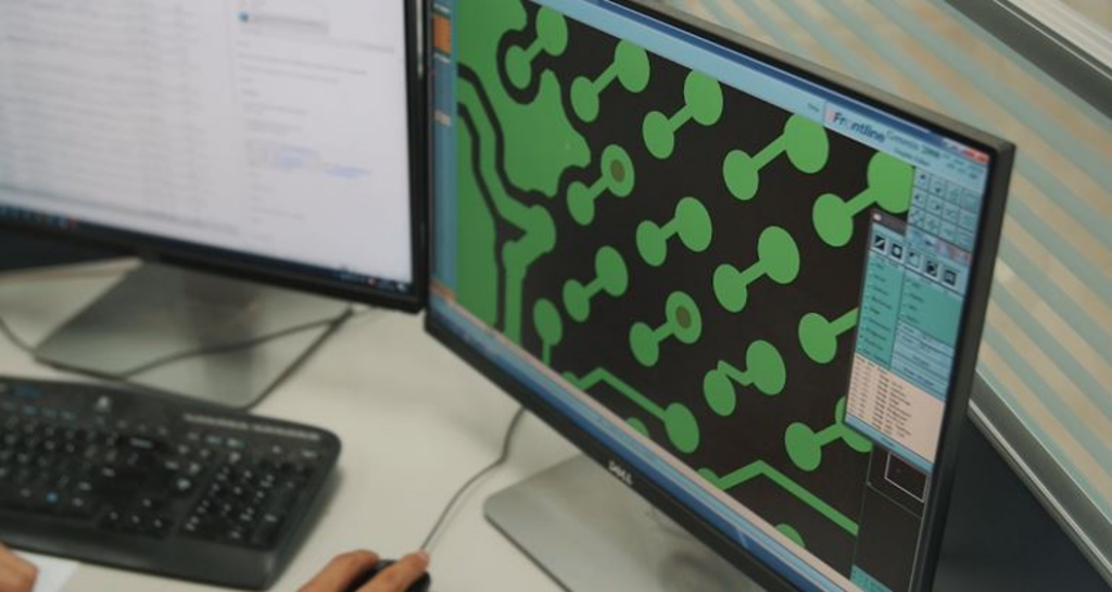
4 - Artwork Printing
Each PCB layer is verified and transferred to the Printing artwork machine. We have one artwork for each layer: inner, outer, solder mask, legend printing, and also special layers like vias, peelable mask, carbon, etc. All those artworks can be used for thousands of panels.
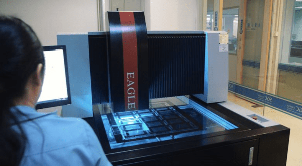
5 - Artwork Control
Each PCB layer is verified and transferred to the Printing artwork machine. We have one artwork for each layer: inner, outer, solder mask, legend printing, and also special layers like vias, peelable mask, carbon, etc. All those artworks can be used for thousands of panels.
Other steps
Welcome
To ensure compliance with European data protection regulations, please verify you are in Europe.