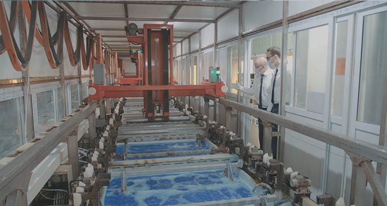
The chemical deposition of copper, also called electroless copper, creates the electrical connection between the inner layer and the outer layer.
1 - STANDARD CLEANING
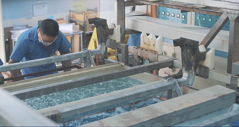
Before depositing the chemical copper, the board must be clean. For the standard process, the first baths will clean up and remove all residue from drilling.
2 - PLASMA CLEANING
For high-tech products, the plasma process is preferable: capable of removing harder residues such as polyimides, High Tg-FR4, Teflon and RF Microwave materials. This optional process provides excellent roughness and wettability for chemical deposition of copper.
3 - PALLADIUM PLATING
Several chemical treatments exist to obtain conductive holes, we can use copper, palladium, graphite, polymer, according to the PCB technology in creation. The boards are immersed in a palladium bath also known as an activation bath to deposit a thin coat of palladium.
4 - COPPER PLATING
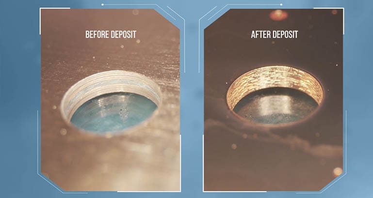
The panels are constantly moving through the bath to remove potential air bubbles that may have formed inside the holes. The palladium acts chemically so that a 1 to 3-micrometers deposit of chemical copper is attracted onto the entire surface of the panel and the recently drilled holes.
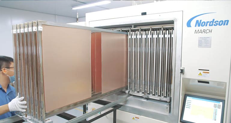
5 - CONTROLS
The control is carried out at the end of this process, mainly, a backlight test is performed to check the porosity and coating of the copper.
Other steps
Welcome
To ensure compliance with European data protection regulations, please verify you are in Europe.