
Leiterplattendichte
Die Dichte ist das Verhältnis von Leiterbahnen, Löchern und Pads pro Flächeneinheit (mm², inch² usw.). Wenn es nur wenige Leiterbahnen gibt, ist die Dichte kein Thema. Aber die moderne Dichte erfordert moderne Lösungen und jeden Tag verlangen die Kunden und die Fabriken nach kompakteren und komplexeren Designs, was vor allem auf die Bauteiltechnologien zurückzuführen ist. Je höher die Dichte, desto komplexer ist die Leiterplatte.
Die Herausforderungen für die Produktion
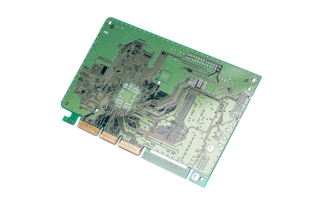
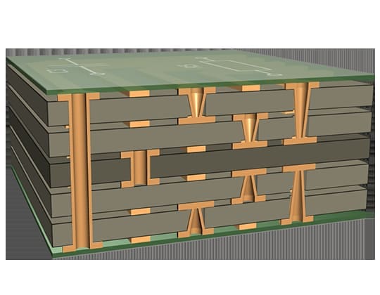
Mit dem Fortschritt und der Miniaturisierung der Elektronik ist die Nachfrage nach HDI-Leiterplatten drastisch gestiegen, aber die Erhöhung der Dichte auf einer Leiterplatte ist eine Herausforderung – vom Design bis zur Produktion. Die Abstände zwischen den Leiterbahnen betragen bis zu 65µm. HDI-Leiterplatten bestehen aus mindestens 4 Schichten und können bis zu 24 Schichten umfassen, die durch Löcher und Durchkontaktierungen miteinander verbunden sind, was zu ultrakomplexen Designregeln und Produktionsprozessen führt.
Während das Design für die Ingenieure mit ihrer Software eine Herausforderung darstellt, besteht eines der Hauptprobleme in der Produktion darin, die Zuverlässigkeit der beschichteten Löcher zu gewährleisten. Das Hauptproblem liegt in den Durchkontaktierungen und Löchern und der Beschichtung. Um eine gute Integrität der Lochbeschichtung zu gewährleisten, wird das Seitenverhältnis auf 1 begrenzt: 0,8 für Blind Vias, der fortgeschrittene Wert ist 1:1. Standard-Prepregs enthalten außerdem Glasfasern, die für das Laserbohren zu dick sind. Das im Prepreg enthaltene Glas verändert die Laserrichtung und erzeugt eine mittelmäßige oder falsche Formqualität der Laserdurchgangslöcher.
Wichtigste Möglichkeiten
| HDI | Fähigkeiten |
|---|---|
| Anzahl der Schichten MIN & MAX | 4-24L |
| HDI-Aufbauten 1+N+1, 2+N+2 | 3+N+3 und beliebige Lagen |
| Werkstoffe FR4, ..., ETC. | Siehe Tabelle |
| Kupfer Gewicht MIN & MAX | 0,5oz~6oz |
| Mindestspur & Abstand MM | 65/65μm |
| PCB-Dicke MIN & MAX | 0,4-2,8mm |
| Abmessung MAX | 0.457*508mm |
| Oberflächenbeschaffenheit OSEP, ENIG, ETC. | HASL, HASL LF, ENIG, chemisch Zinn, OSP, chemisch Silber, galvanisches Hartgold/Weichgold, Goldfinger, selektives OSP, ENEPIG |
| Mechanischer Bohrer MIN | 0,15 mm |
| Laser-Bohrer MIN | 0,076mm |
Améliorer la conception et la fiabilité des circuits imprimés HDI
Haben Sie Fragen?
Es gibt ein Team der ICAPE Group in der Nähe von Ihnen und Ihrem Unternehmen. Überall auf der Welt sind unsere Geschäftseinheiten mit einheimischen Experten besetzt, die alle Ihre Fragen beantworten können. Kontaktieren Sie uns noch heute!