
36
Business units
6
Laboratories
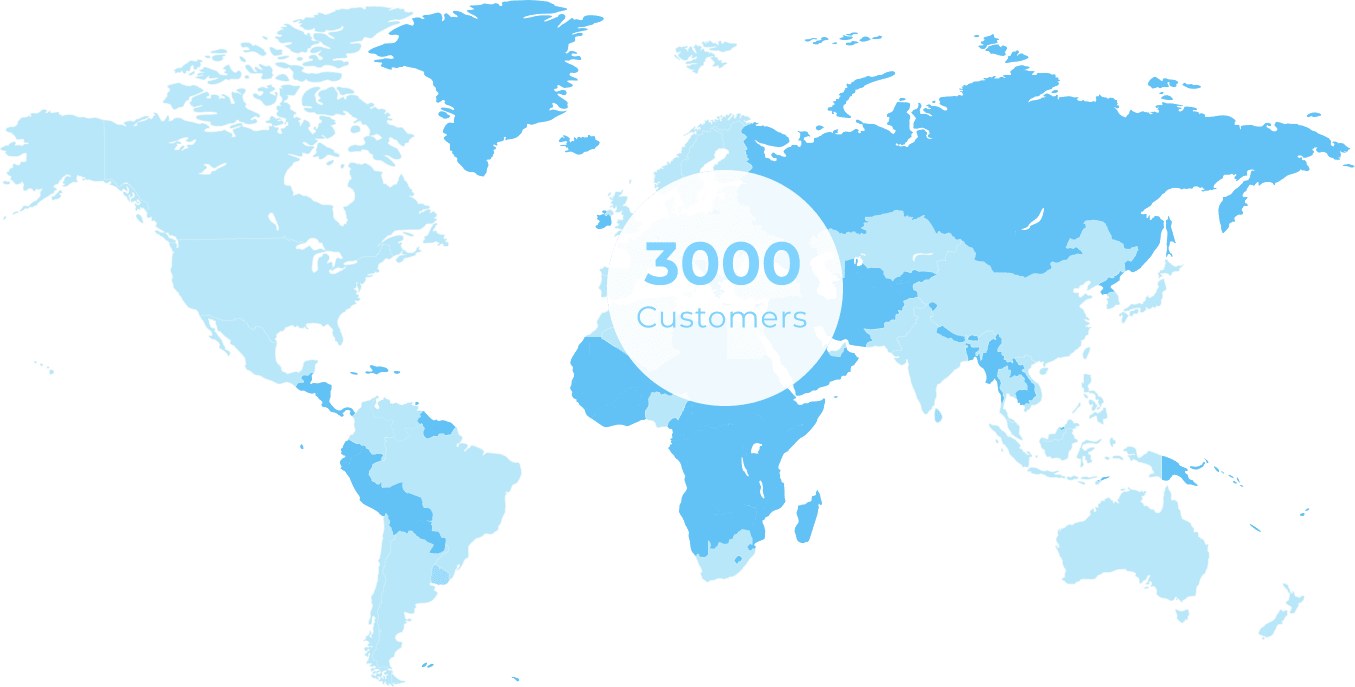
3650
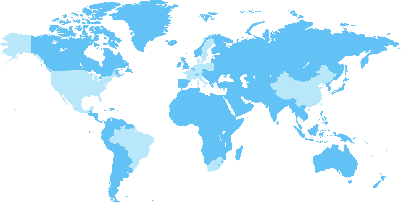
Customers
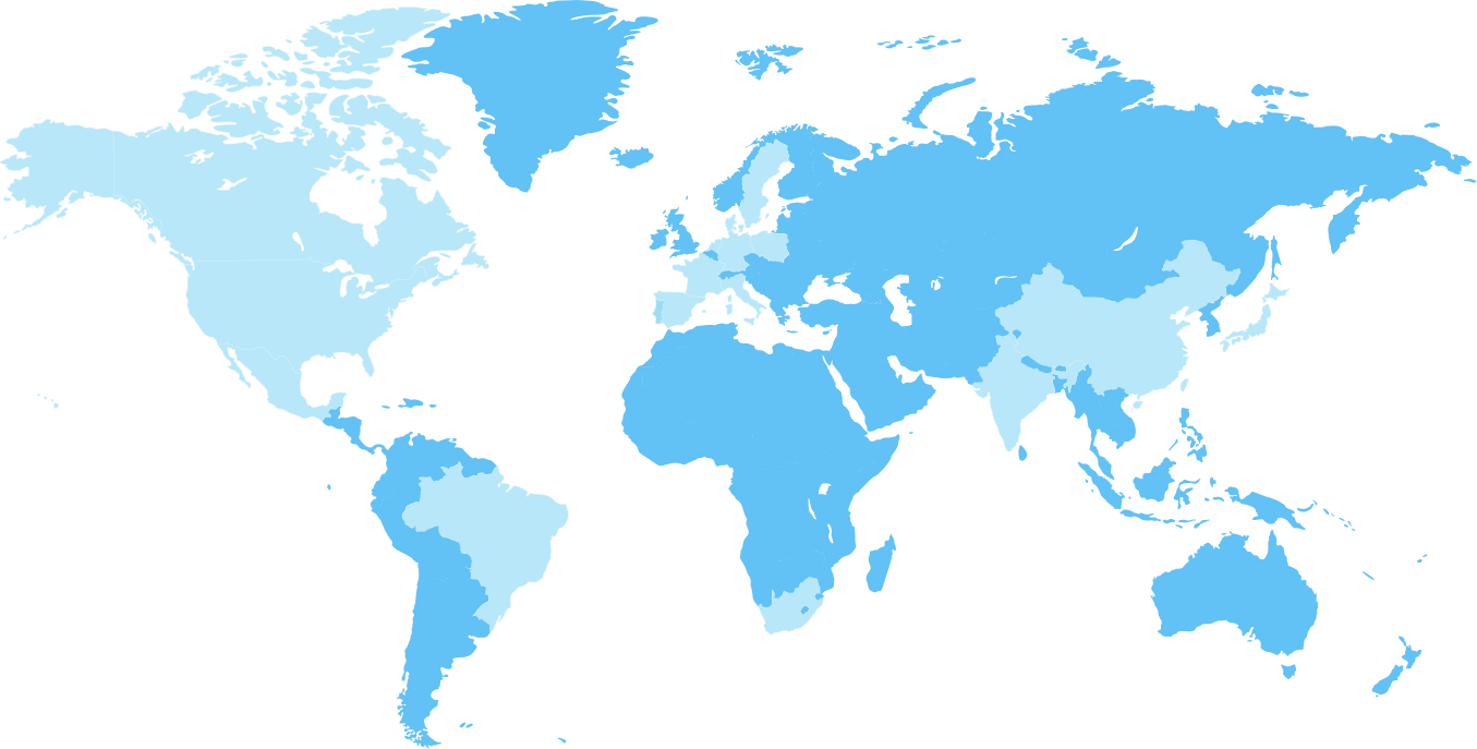
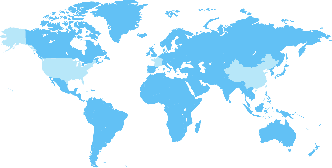
60
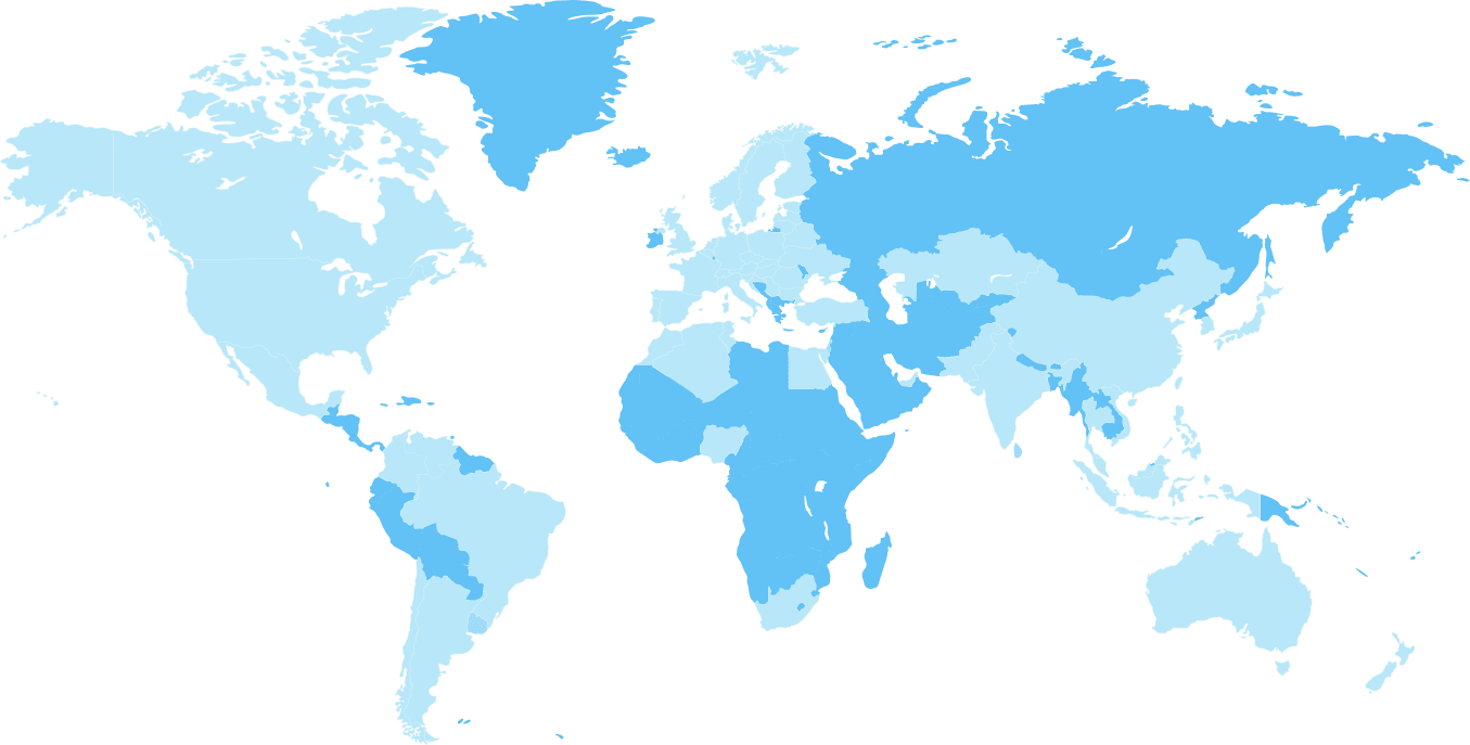
Countries delivered
11
Warehouses
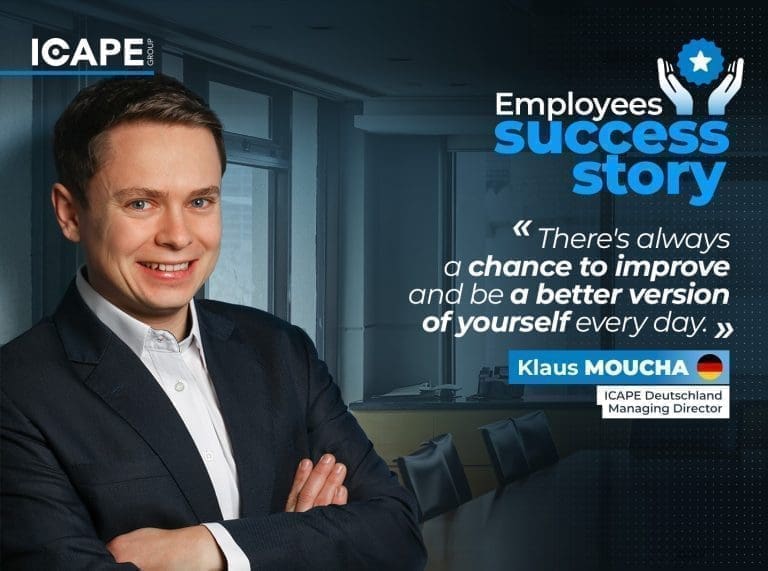
Employees Success Story : Klaus Moucha, a vibrant and dynamic new leader at ICAPE Group
Meet Klaus Moucha, a vibrant and dynamic new leader at ICAPE Group. With his optimism, humor, and unwavering determination, Klaus…
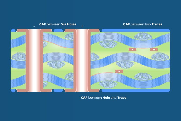
CAF : Understanding Conductive Anodic Filament (CAF) on PCBs
CAF : Understanding Conductive Anodic Filament (CAF) on PCBs Let’s explore a fascinating undesirable aspect of PCBs called Conductive Anodic…
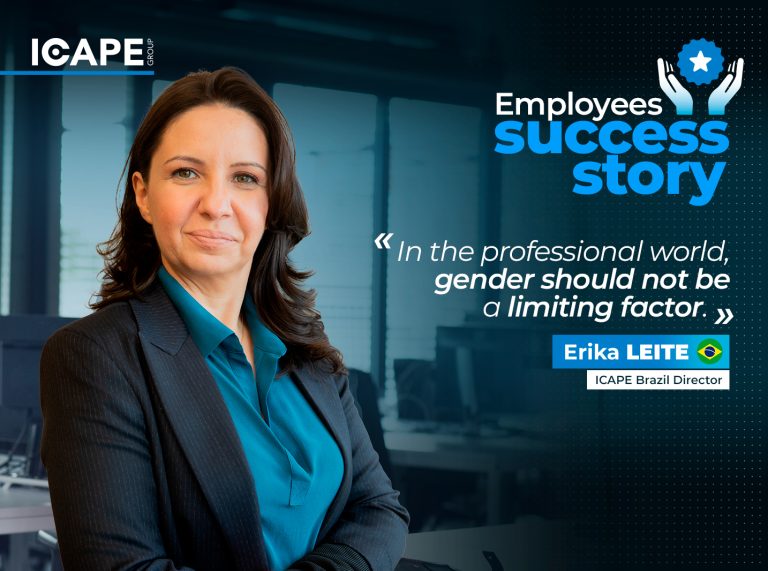
Employees Success Story : Erika Leite, ICAPE Brazil Managing Director
In celebration of International Women’s Day, we are delighted to present an insightful interview with Erika Leite, a passionate and…