
Impedance Control
Electrical impedance is the measure of the opposition a circuit presents to a current when a sinusoidal AC voltage is applied. This cable is a coaxial cable. Instead of a coaxial cable, an antenna can be connected to the device by a cable formed of two round wires spaced apart from a flat plastic strip. As with the coaxial cable, the dimensions and materials of this wire are carefully controlled to give it the correct electrical impedance.
A TV antenna has a “natural” impedance. For Radio Frequencies (FR), the transfer of the maximum signal power from the antenna to the cables requires that the impedance of the cable matches the impedance of the antenna. In addition, the impedance of the TV must match the impedance of the cable.
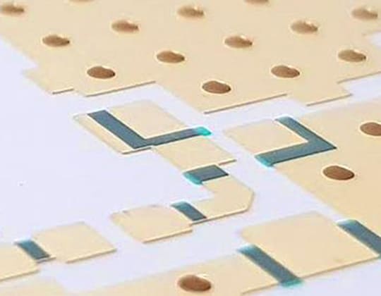
Although we have to focus on wire interconnections, the same considerations apply to signal transfer through traces on a PCB. As recently as 1997, only the then high-speed exotic devices required PCBs with controlled impedance. These amounted to perhaps 20% of the manufactured PCBs.
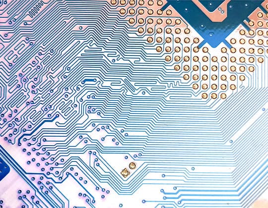
In 2000, about 80% of all multilayer PCBs were manufactured with traces of controlled impedance. These included boards for all types of technologies including :
– Telecommunications
– Video signal processing
– High-speed digital processing
– Real graphic processing
– Process control
Most homes today have a great number of low-cost applications of these technologies, for example:
– Modem, phones, satellite TV
– GPS
– Radar
– Video games
– Low-cost PC
– Auto engine control modules
What kind of impedance design can we meet on PCB?
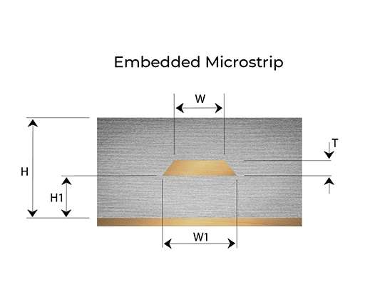
Embedded Microstrip
An embedded microstrip transmission line, similar to microstrip, is made up of a conductor, usually copper, of width W and thickness t routed over a ground plane that is wider than the transmission line itself and separated by a dielectric substrate of thickness H1.
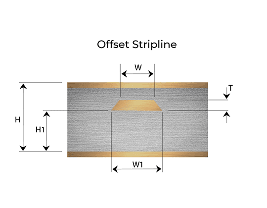
Offset Stripline
In the offset Stripline configuration, the signal trace is sandwiched between two planes and may or may not be equally spaced between the two planes. This construction is often referred to as Dual Stripline.
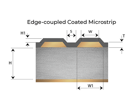
Edge-coupled Coated Microstrip
The edge-coated microstrip is a differential configuration in which there are two traces of controlled impedance on the surface, coated with a resist and a plane on the other side of the laminate.
Edge-coupled Offest Stripline
Edge coupled offset Stripline is a differential configuration with two controlled-impedance paths sandwiched between two planes. The traces are staggered, but they could be halfway between the planes (2H1 + T = H)
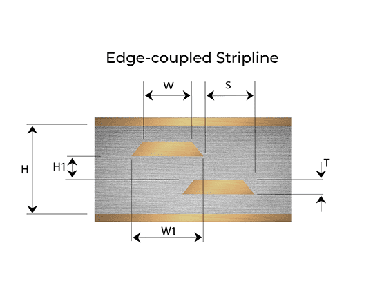
Edge-coupled Stripline
This differential configuration has two traces separated by a laminate and sandwiched between two planes. Although the diagram shows the offset of the traces, the manufacturing objective is to have the traces without offset, i.e, one must be directly above the other
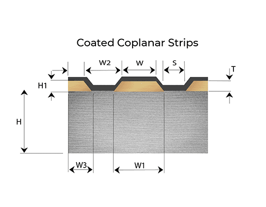
Coated Coplanar Strips
In this Coated Colplanar Strips configuration, there is a single trace of controlled impedance with two ground traces of a specified width (W2/W3) on each side. All the traces are coated with resist.
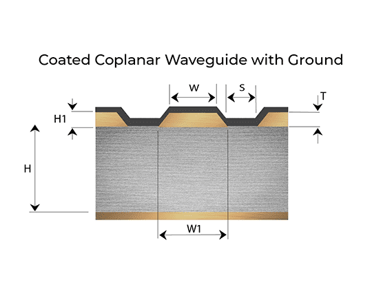
Coated Coplanar Waveguide with Ground
The coplanar waveguide has a single trace of controlled impedance with planes on each side (or very wide ground traces), a continuous plane on one side and a laminate only on the other.
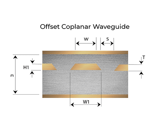
Offset Coplanar Waveguide
The Coplanar Waveguide is similar to the above configuration, with the exception that there are planes on both sides of the laminate and a plane on the same layer as the controlled impedance trace.
How to Control Impedance?
What is a test coupon?
Any questions?
There is an ICAPE Group team close to you and your business. All around the world, our business units are staffed with native experts available to answer all your questions. Contact us today!