Copper can be deposited electrolytically on the board with two processes : Panel and Pattern process.
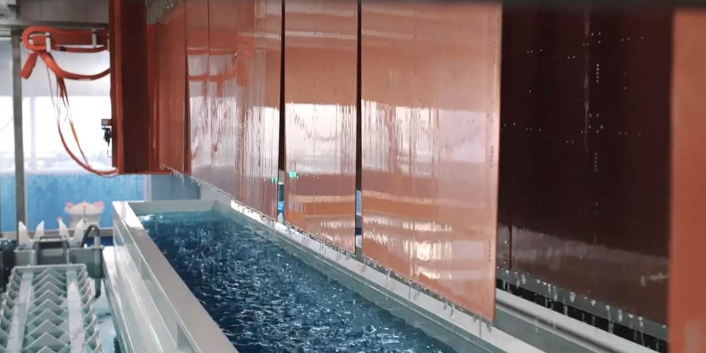
1 - PANEL PLATING
The copper is electrolytically deposited over the entire surface as well as inside the holes to improve flatness and distribution. Electrolytic copper creates electrolysis, which is a flow of electric current through a liquid that causes chemical changes. After several baths of 3 min each, electrolysis is created, the copper in the bath acts like an anode and the boards like a cathode.
2 - CONTROL
Copper is now thicker and more reliable with around 10 to 13 micrometers of copper. The next step for these boards will be the Outer Layer Imaging.
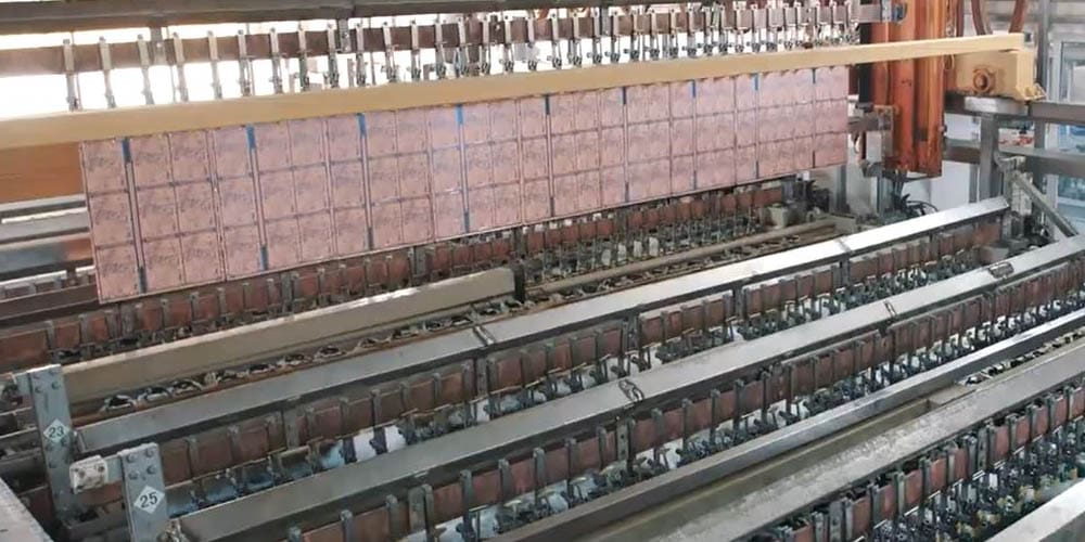
3 - PATTERN PLATING - COPPER DEPOSITION
The copper is deposited electrolytically, but in much greater quantities. To create a good connection and a good conductivity between the holes, the boards need at least 20 to 25 micrometers of copper inside the wall holes according to IPC standards. The copper, acting as an anode, is deposited on the boards during a 60-minute bath.
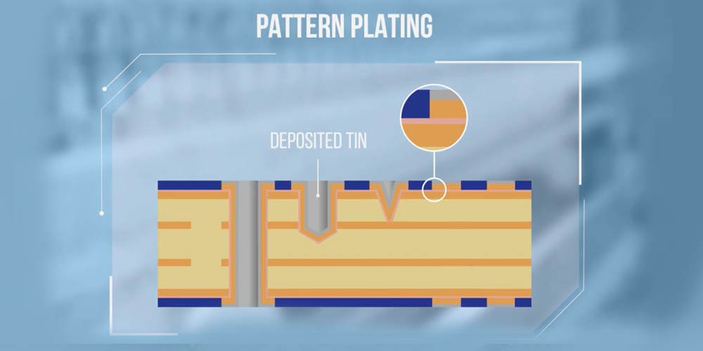
4 - PATTERN PLATING - TIN DEPOSITION
After a rinsing bath, the boards are immersed in the electrolytic tin which covers all the copper with a coat around 1 to 3 micrometers. The tin is essential to protect the copper during the etching process.
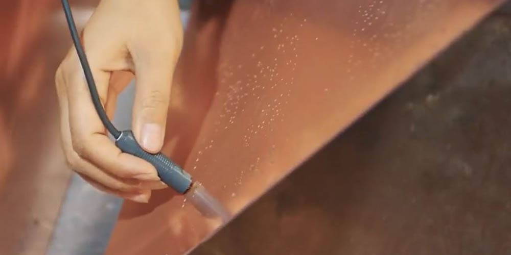
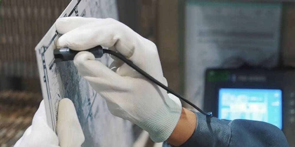
5 - CONTROL
Once they are completely covered, they are test with a non-destructive method to check the thickness of the coat.
Other steps
Welcome
To ensure compliance with European data protection regulations, please verify you are in Europe.